 Luke Valenty
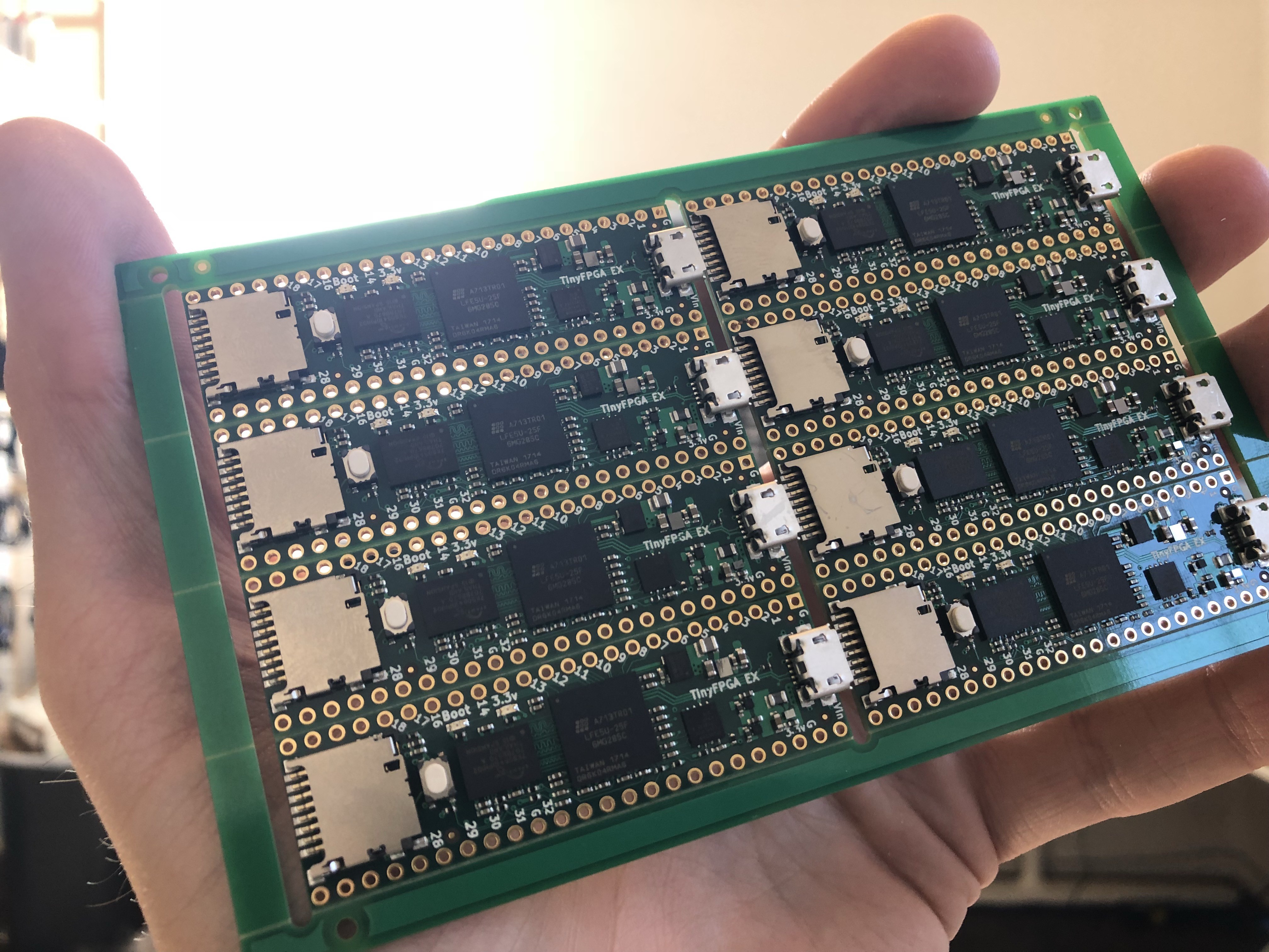
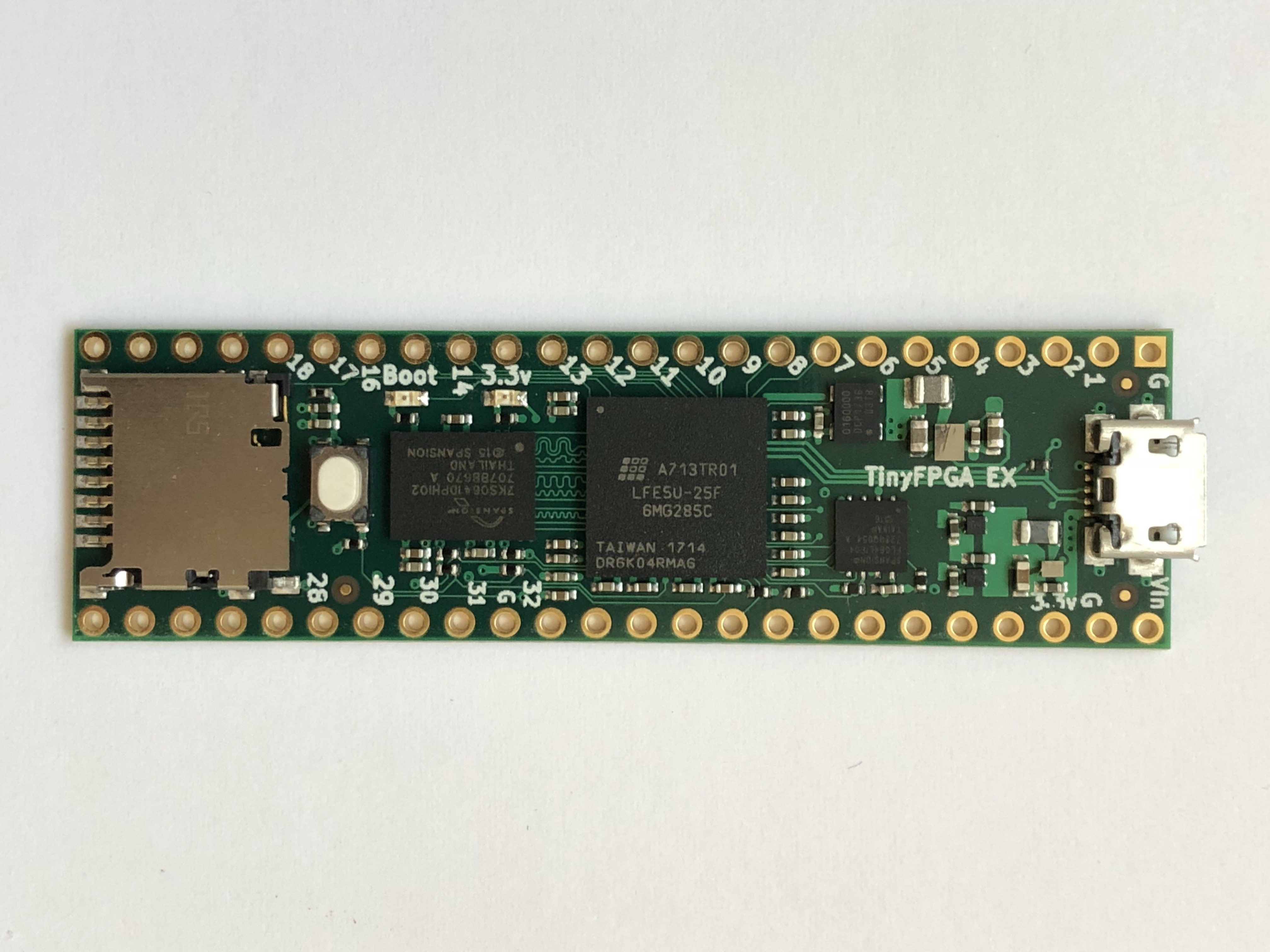
After months of waiting the TinyFPGA EX prototypes arrived a few days ago! I was so thrilled to finally try them out that I forgot to write a Hackaday.io post about it.
The prototype run was for one panel of 8 boards.
The first thing I did was check the bare PCBs that were sent alongside the assembled boards. It looked like there were vias missing. An inspection with my USB microscope seemed to confirm this.
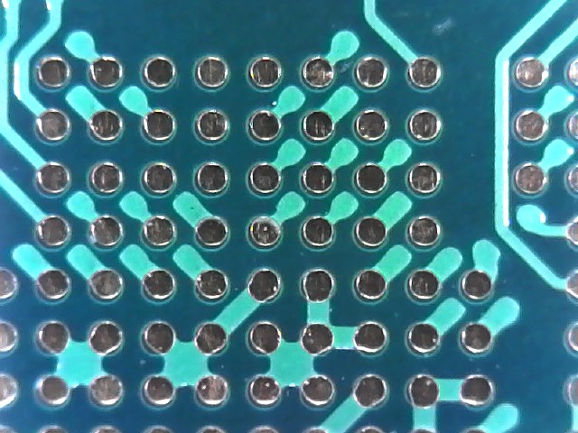
I took out my multimeter to check the resistance between various pads and the external pins. Despite looking like there are missing vias, their is a reliable connection between the pads and their respective pins on the board. I'm not sure why the vias aren't visible. Maybe the plating filled in the small holes completely?
While I had the bare PCBs under the microscope I took a look at the pads for the power supplies. The two switching supplies are tiny BGA packages. The 1.1v supply can supply up to 5 amps of current! However, the inductor I choose is rated for up to 4.3 amps.
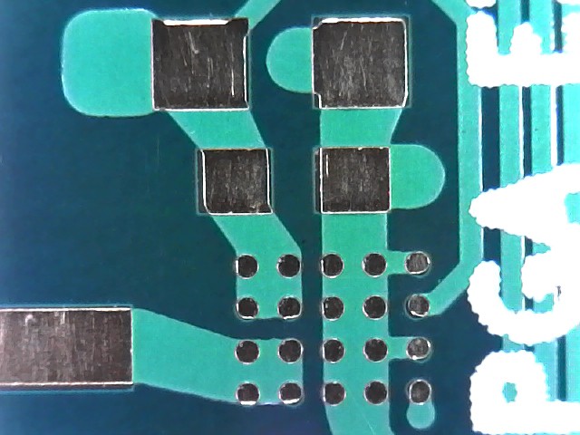
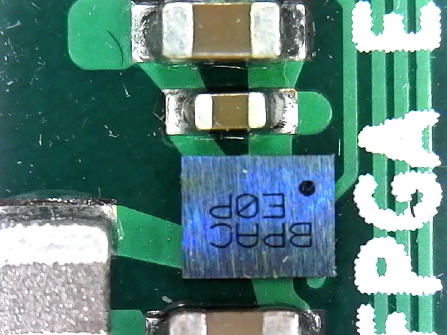
There are also a couple of linear LDO regulators that have a unique footprint. They are super tiny.
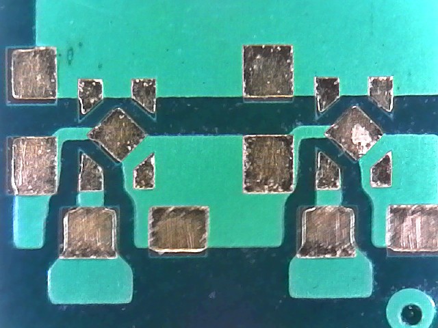
We can see that the PCBs very good quality considering the tiny size of the components and traces. Afterwards I wanted to take a look at the power supplies as assembled on the board.
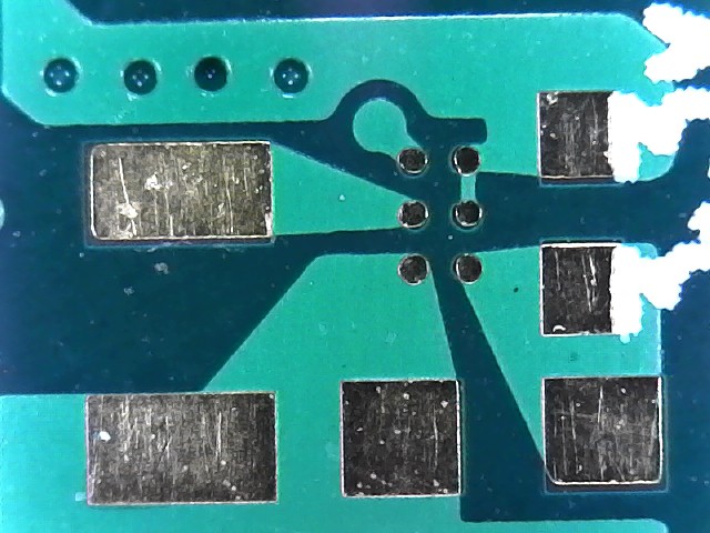
Grey surface mount passive in the corner is the inductor for the switching power supply in the center. The brown components are the input and output capacitors.
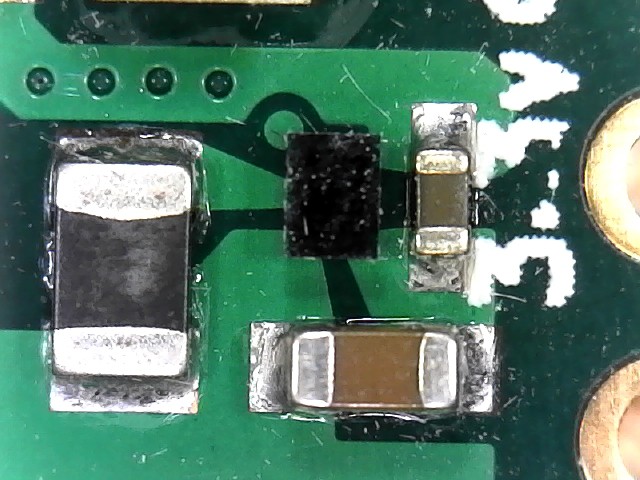
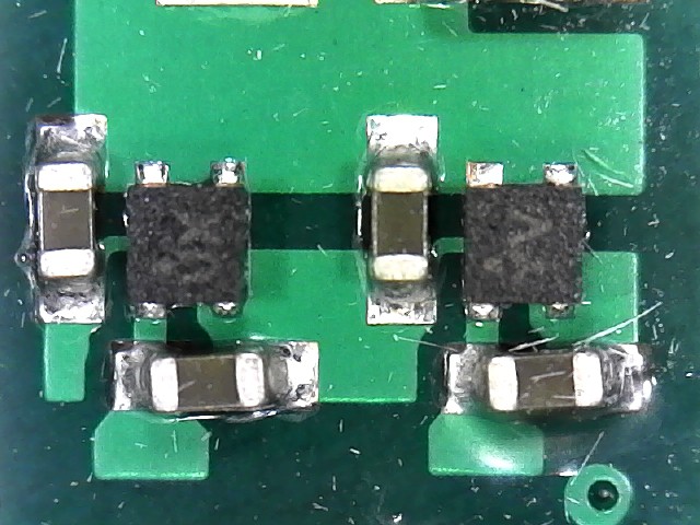
The two switching supplies appear to be assembled properly and the footprints are good.
The linear LDOs are each capable of sourcing 300mA of current. They are used for the HyberRAM and the VCCAUX of the FPGA. After inspecting various components I broke out a few boards to start the process of bringing up and debugging a new FPGA board.
Before powering the board on, I wanted to make sure I wasn't going to let out the magic smoke. I measured the resistance between the ground and various supply pins. They were all high enough resistance that dangerous shorts were very unlikely. I was confident enough to apply Vin.
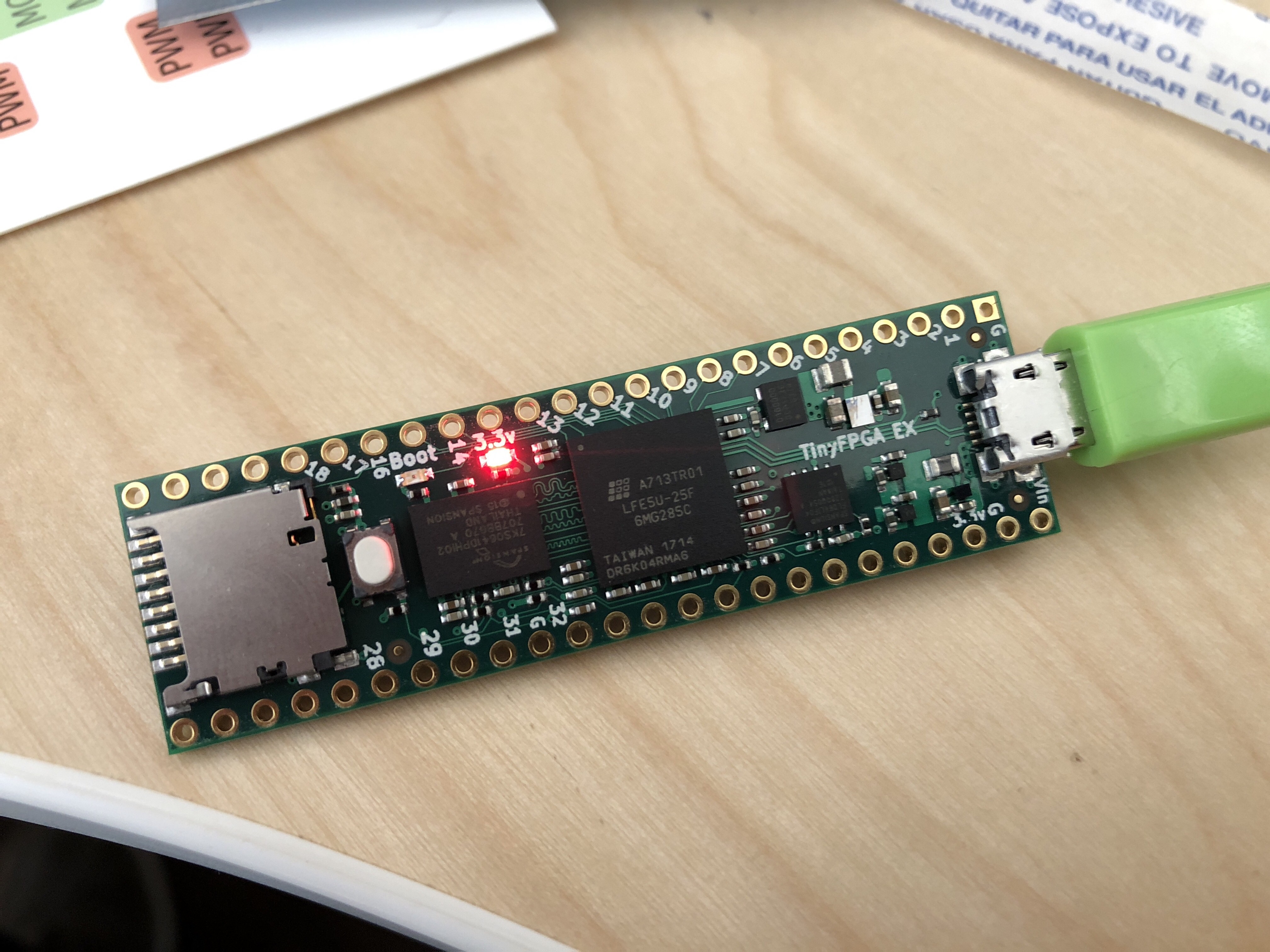
It worked! Well, at least the 3.3v switching power supply worked well enough to light up the 3.3v power indicator LED. I checked voltage levels of all the power rails and they were spot on. Another good sign. Next step is to see if the FPGA itself is functional. To do this I would want to connect the JTAG interface to the Lattice programming cable. The JTAG test points are on the bottom of the board and I didn't have a test-jig setup yet so I would need to solder some cables to the test points.
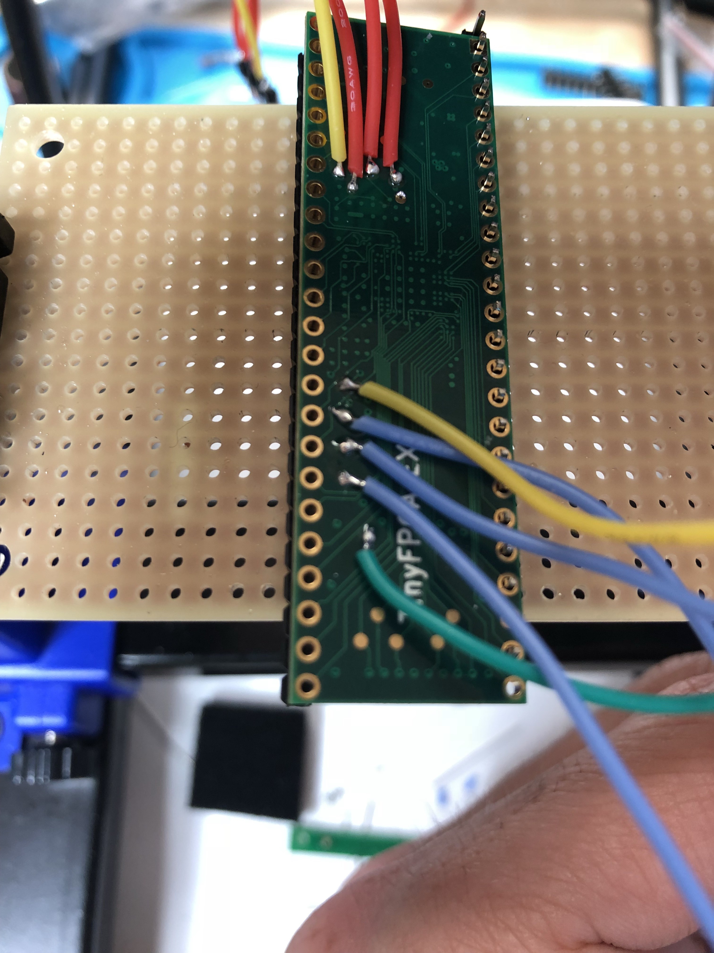
In addition to the JTAG port, the flash SPI interface is also on the bottom. I connected headers to both of these ports so I could spy on the configuration sequence. Running a simple ID code read on the Diamond Programmer application I got a sign of life from the FPGA!
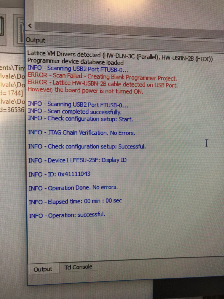
This is a very good sign. The basic functionality of the FPGA is working. I discovered I could also read out the status register from the FPGA.
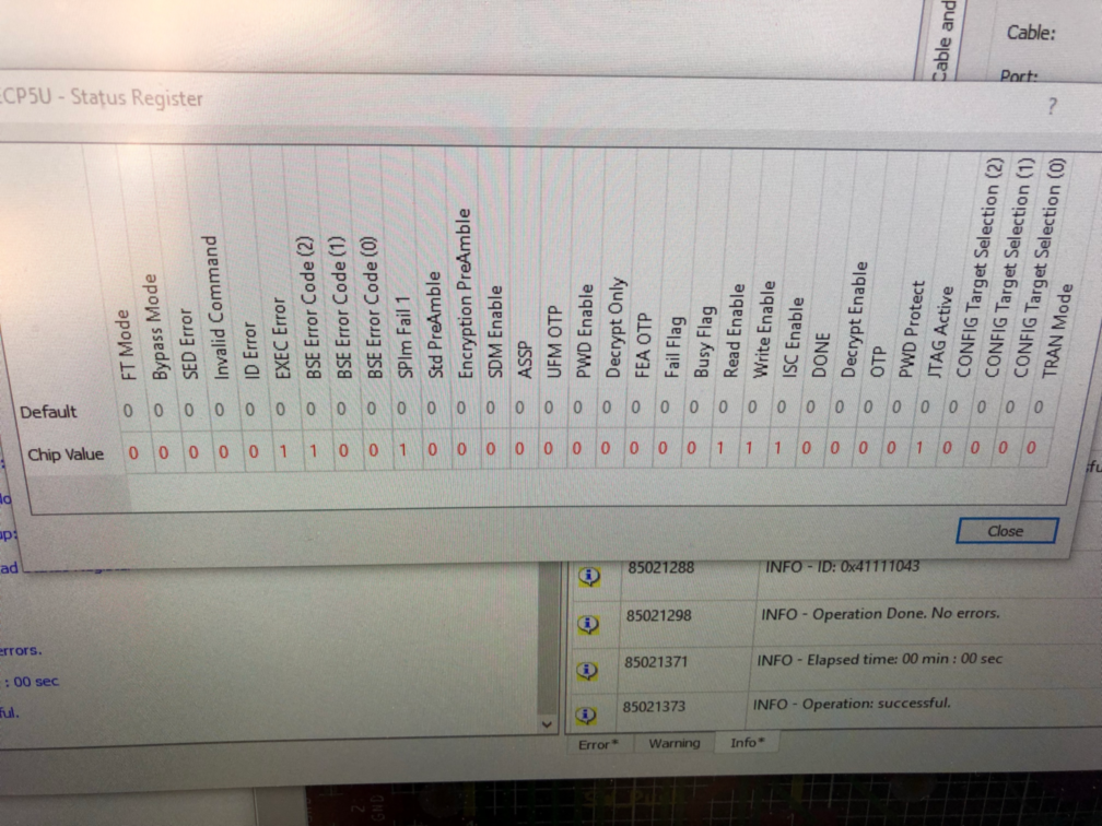
The status register reported an error. After reading the Lattice documentation I decoded the message. It translates into the following English: "I couldn't load a configuration from SPI flash. The data stored there didn't have a valid preamble." Very cool. The ECP5 FPGA can be configured in multiple different ways. I had setup some pull-up and pull-down resistors in a few pins to tell it to pull its configuration from flash. It appears to be working! Now I needed to load a valid bitstream onto the SPI flash. To do this, I wanted to use my USB bootloader from the TinyFPGA B2 project. This means I would need to port the bootloader over.
It was actually a lot easier than I expected. The FPGA programmed over JTAG just fine and bootloader was visible and functional over USB right away.
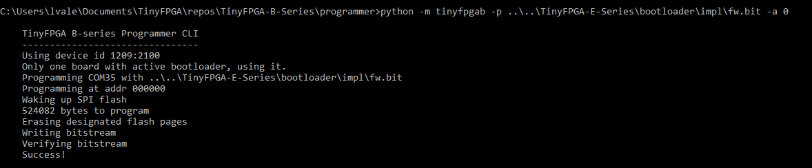
The ECP5 FPGAs do have a few oddities that tripped me up. The bootloader needs to use the SPI pins to program the SPI flash. Lattice Diamond wasn't letting me use the SPI CLK pin for a user IO. That was very odd. For a moment I thought I would have to connect another pin to the SPI CLK. Going over the documentation for the umpteenth time I discovered there is a special primitive I could use to drive the SPI CLK from user logic. This is exactly what I wanted. Except it didn't work. More debugging. Some head banging. More debugging. Ah-ha! I looked up the RTL graphical representation from the Synplify synthesis tool and I had some combinatorial loops feeding into the user SPI CLK mux. Once these two loops were gone the flash was able to be programmed over the USB bootloader.
Would it boot? It didn't take long to find out. I unplugged the board to ensure the volatile config RAM was cleared and plugged it back in. Nothing. Wait...the bootloader LED is flashing! The ECP5 FPGA is much larger than the iCE40 FPGA I had been used to in the B2 and BX boards. It had a lot more data to transfer, and the bitstream was configured for the default 2MHz clock. It was easy enough to increase this to 38MHz and now the boot speed is imperceptible to the human eye.

You might notice the blue bodge wire attached to the reset button. Unlike the iCE40 FPGAs, the ECP5 FPGAs do not support a WARMBOOT primitive. This means that the user logic running in the ECP5 FPGA cannot directly tell the FPGA to reconfigure itself to a specific image. I really should have known this before I ordered the prototypes. It was a big oversight.
Instead of the WARMBOOT primitive, the multiboot bitstream image itself contained the information on which image to load next. To trigger a reconfiguration to the next image, either the PROGRAMN pin on the FPGA has to be pulled low, or a REFRESH command has to be sent on the external JTAG port. It was fairly simple to connect a bodge wire from a user IO pin to the PROGRAMN pin. Now the bootloader is 100% functional on the TinyFPGA EX prototypes.
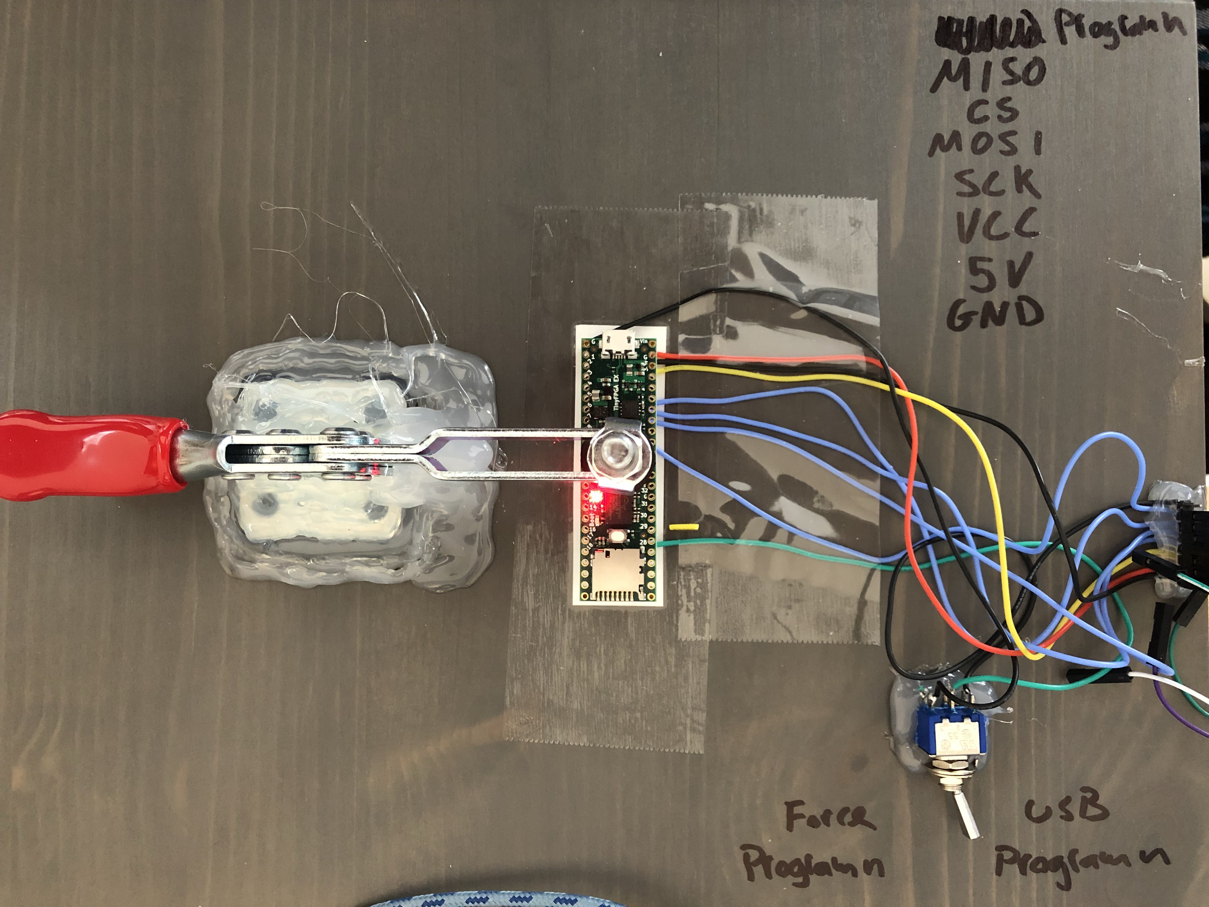
I was eager to bring all of my prototypes up to par so I built a simple programming jig to program the SPI flash directly.
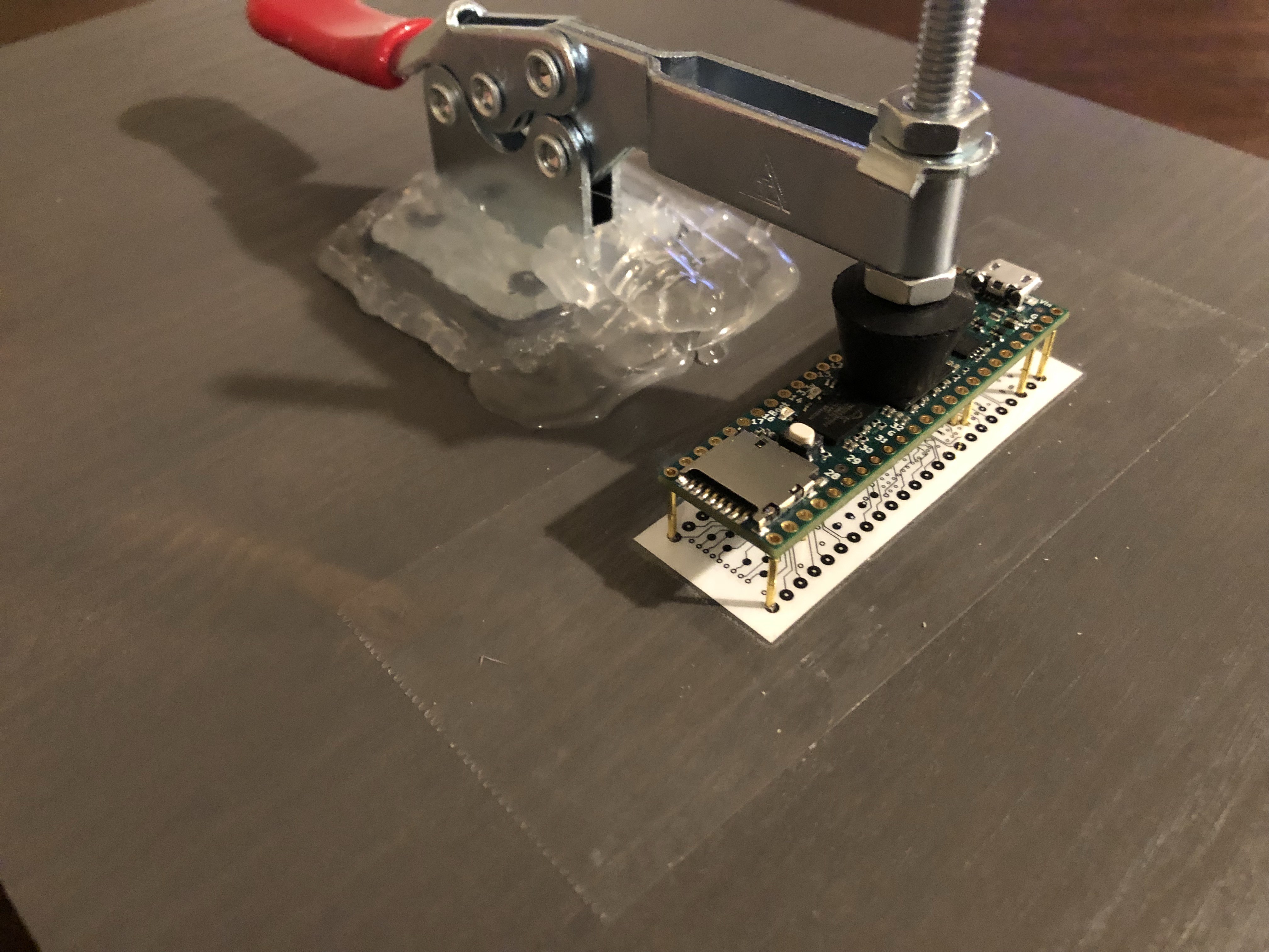
The jig was very simple. Just enough pogo pins to keep the board stable while clamped and program the flash. I broke out the rest of the prototypes and filed their rough edges.

All the prototypes were programmed with the bootloader.
The next step for these boards is to implement some fun designs on them. Something that takes advantage of the HyperRAM and micro SD card slot would be nice.
Follow the project for updates including the eventual details on ordering a production unit.
Discussions
Become a Hackaday.io Member
Create an account to leave a comment. Already have an account? Log In.
Is this project still alive? It seems to have been quite a long time since the prototypes were looking really promising.
Are you sure? yes | no
Beautiful! But where's the USB-C gone? :(
Are you sure? yes | no
Very cool. Reminds me of the Flea Ohm FPGA but 1/2 the size.
Are you sure? yes | no
This really cool, I have not worked with FPGAs yet but I plan to use this to learn. Looks like it might be a good choice.
Are you sure? yes | no
Fantastic work! I cannot wait to get one to explore.
Are you sure? yes | no
So Awesome, good work with your prototypes ! :)
Would it be possible to make the BX-MKII with hyper ram and microSD card on the bottom ?
Are you sure? yes | no