Close
0%
0%

Reverse Engineering Soneplex SPX-MPU SBC

Reverse engineering logs for salvaged MC68302 based SBC

Similar projects worth following
ADC Communication's SPX-MPU board is a MC68302-based controller board for the Soneplex communication product line. This board was phased out around 2005 and large number of them were available on eBay as surplus/salvaged boards. They are still available today (2017), although at a higher price of $15-25 USD.

About 10 years ago I purchased several boxes of salvaged SPX-MPU boards, first from a local electronic surplus outlet and once I've determined these boards were functional, I purchased more from eBay. I've had the vision of building an array of acoustic sonar with them. After sitting at the back shelves of my garage for most of the 10 years, I've retired and finally had the time to work on them. I do not have documents about this board other than what I can find on the Web. These are logs of my efforts.

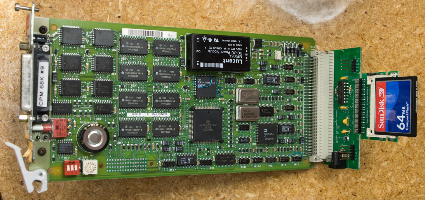
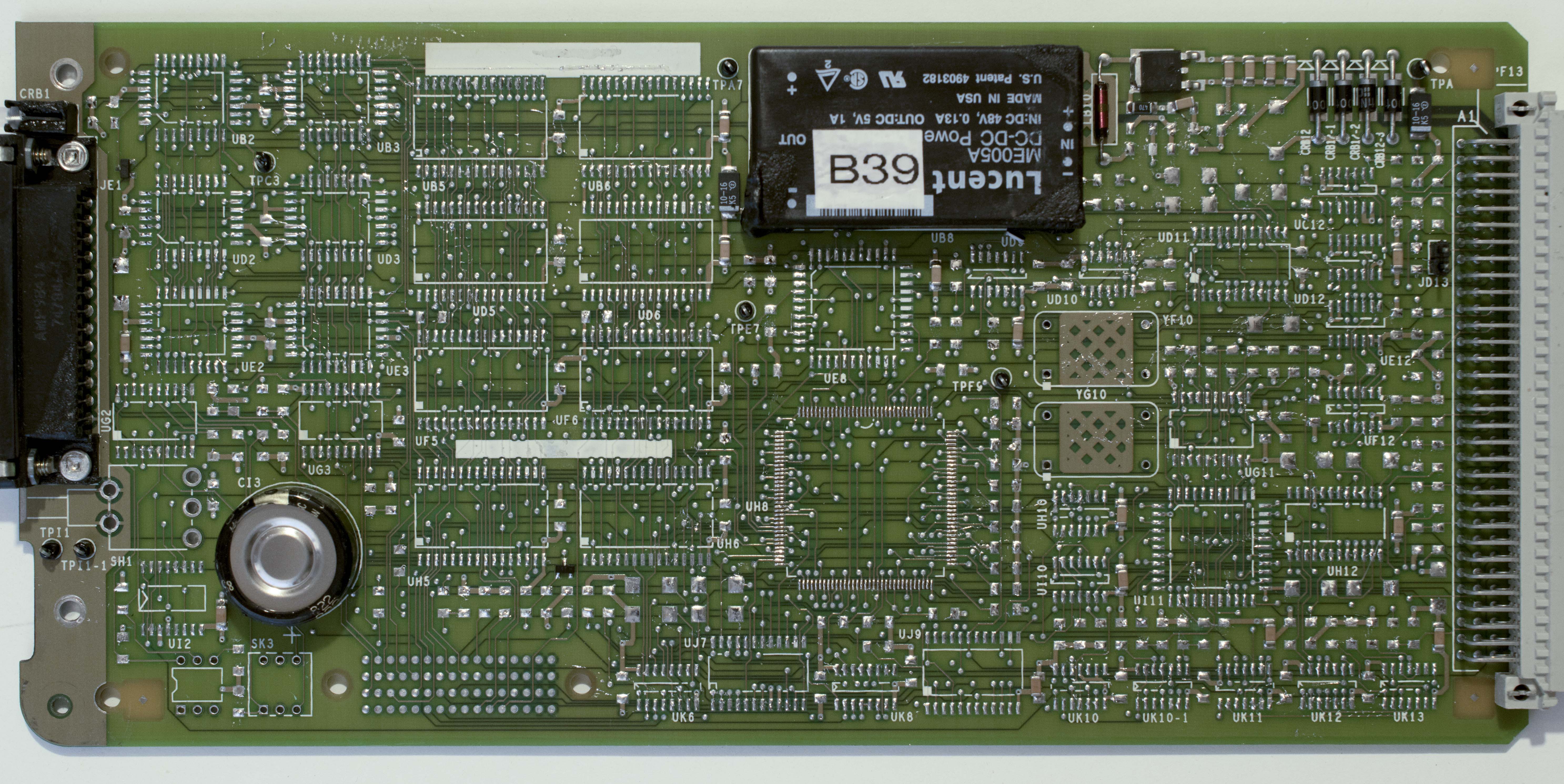
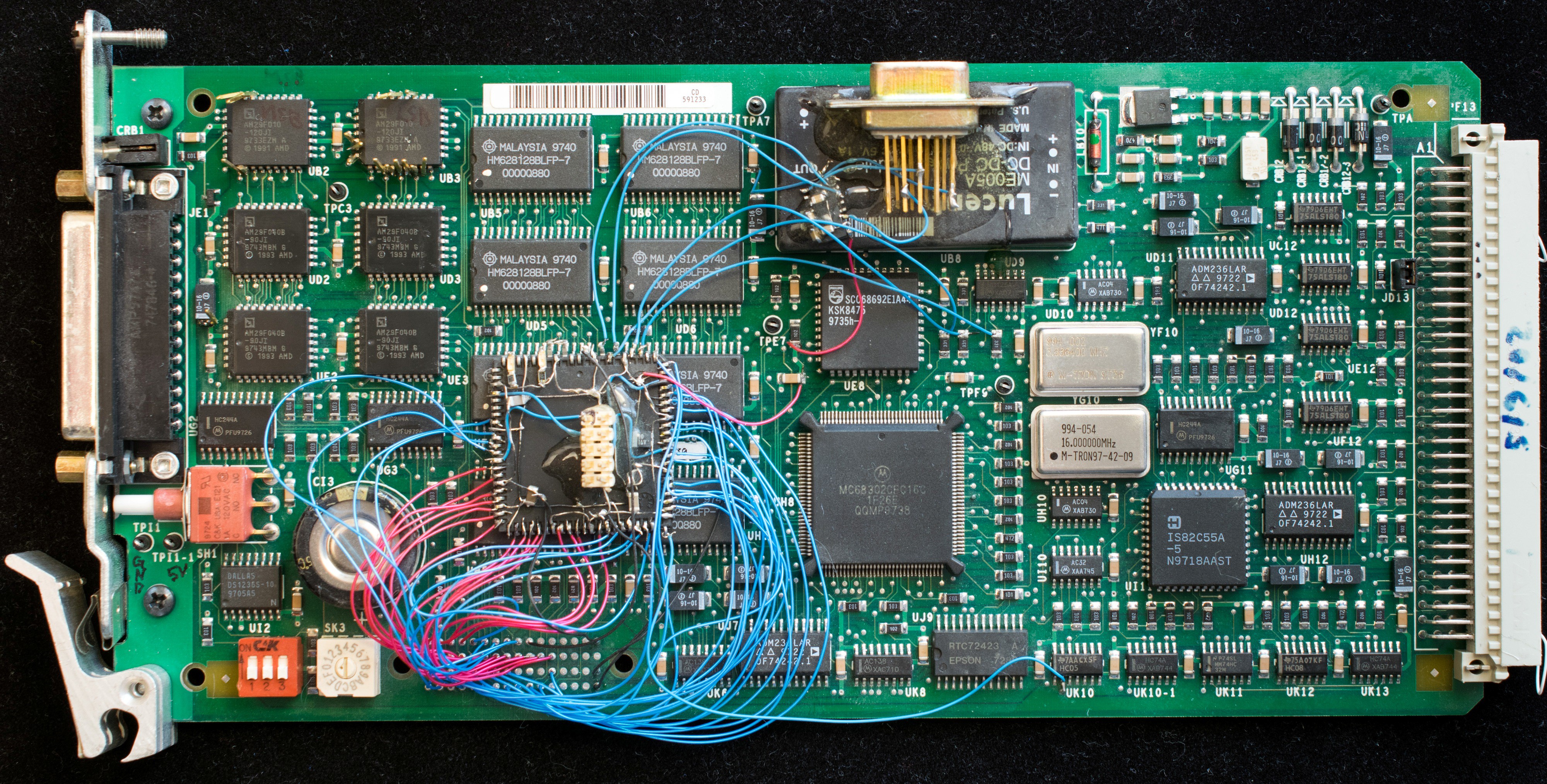
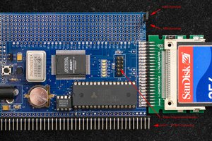
SPX MPU is a general-purpose SBC with the following features:
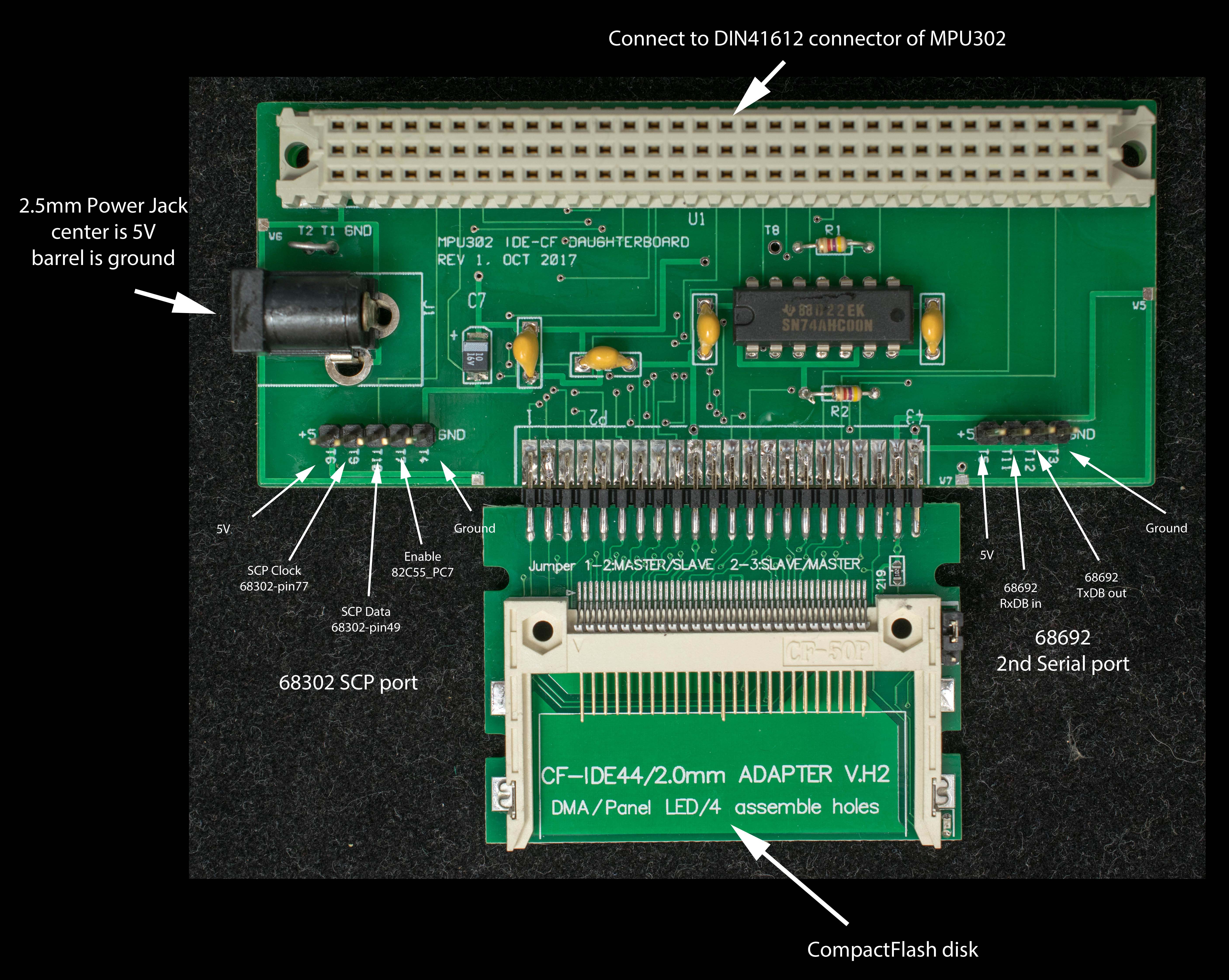
MC68302@16MHz with SPI and 3 SCC,
256K bytes boot flash,
2 Megabytes application flash,
768KB static RAM plus 256KB RAM backed by super capacitor for a total of 1 Megabyte RAM,
82C55 programmable peripheral interface,
68692 Dual UART,
Real time clock,
16 discrete inputs,
Connect to backplane via 96-pin DIN41612 connector,
48V to 5V DC/DC converter  ,
Power consumption at 5V is 250mA nominal.


Chronological list of projects

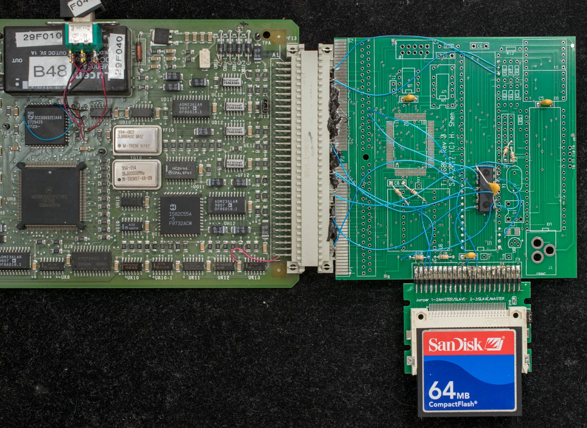
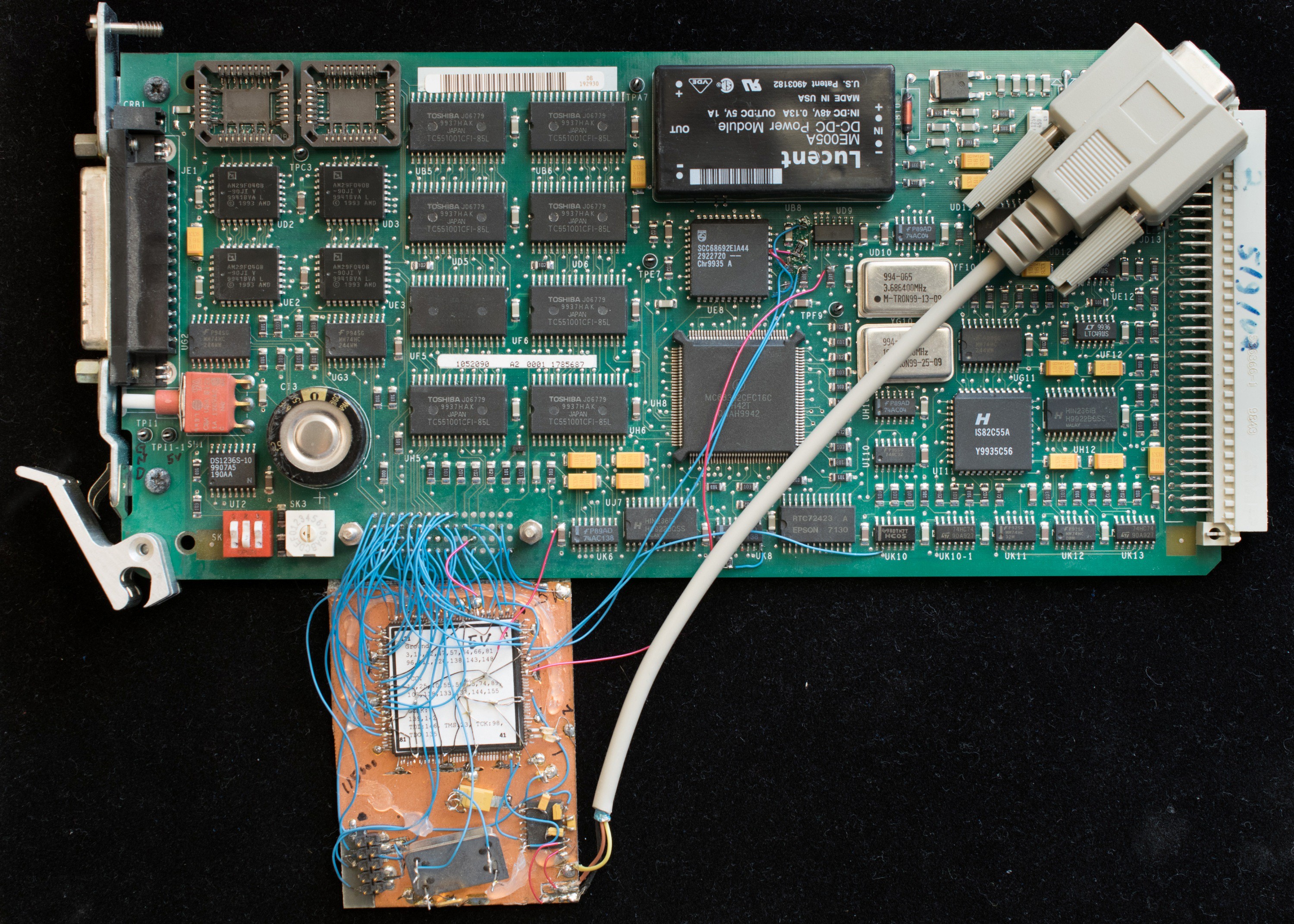
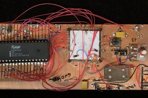
Flashback, exploring the salvaged SPX MPU board

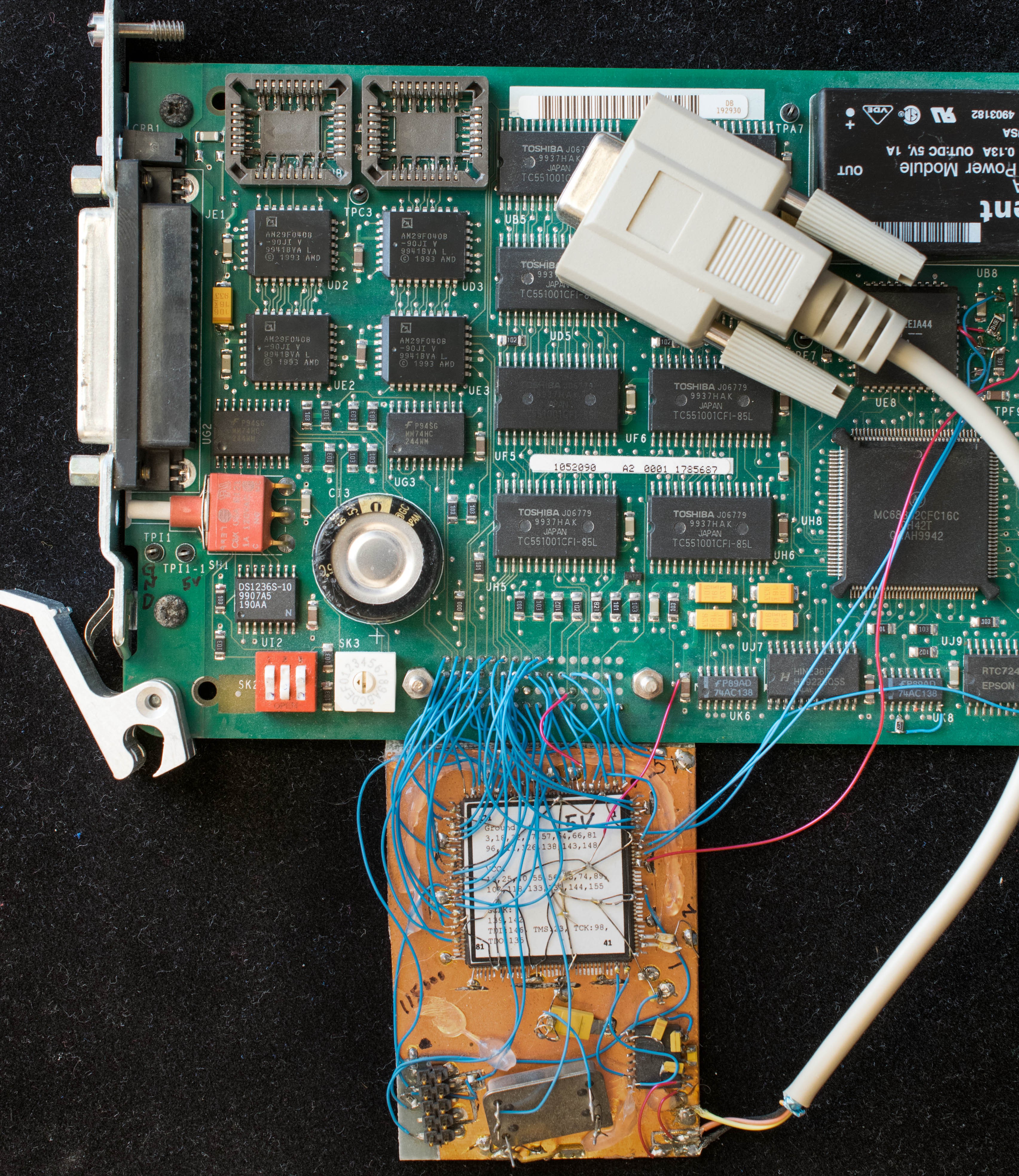
Paradigm Shift, A different way to reverse engineering the SPX MPU board

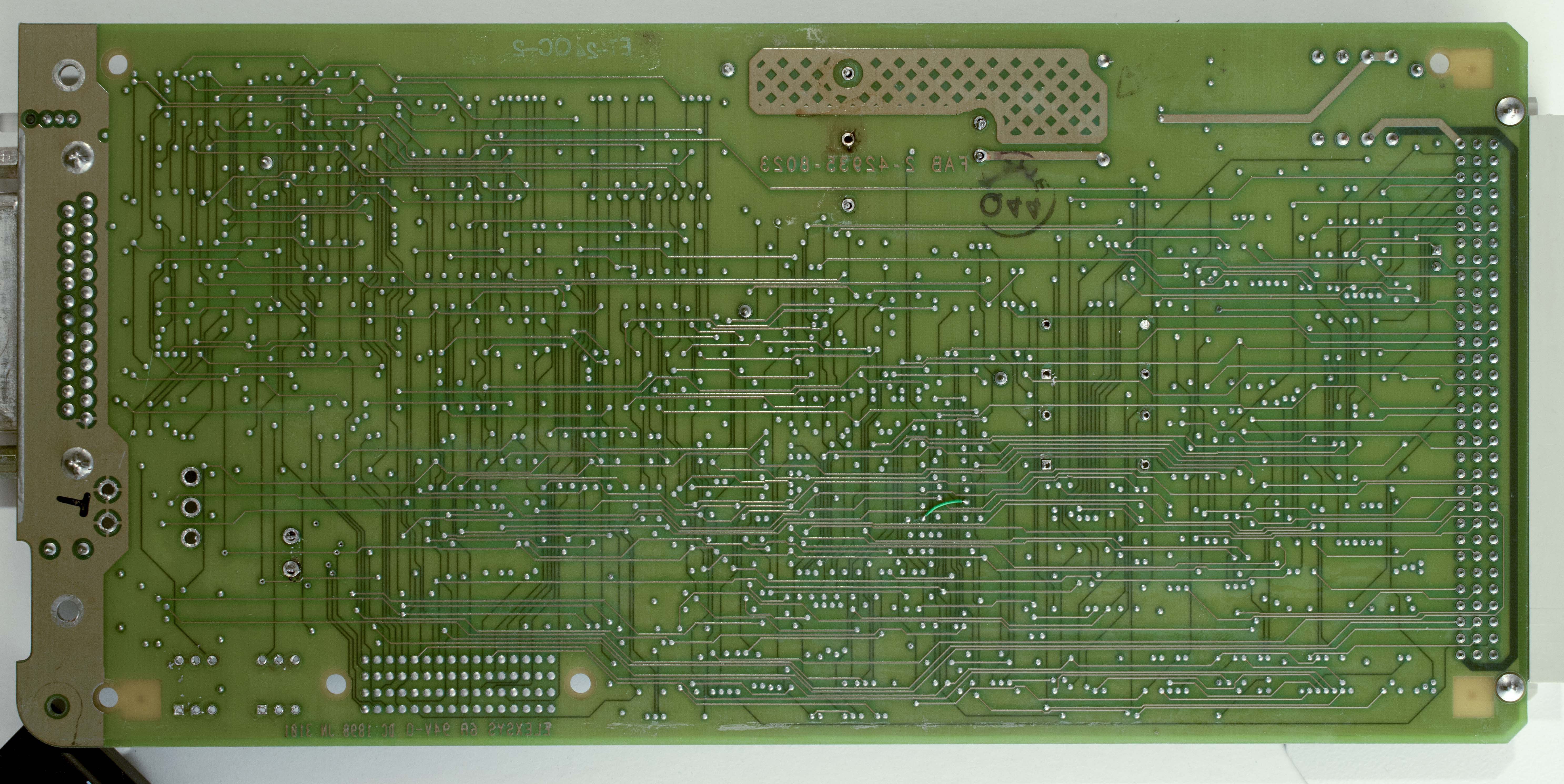
From PC board to Schematic, technique to extract netlist from pc board

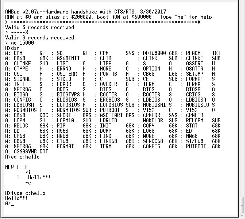
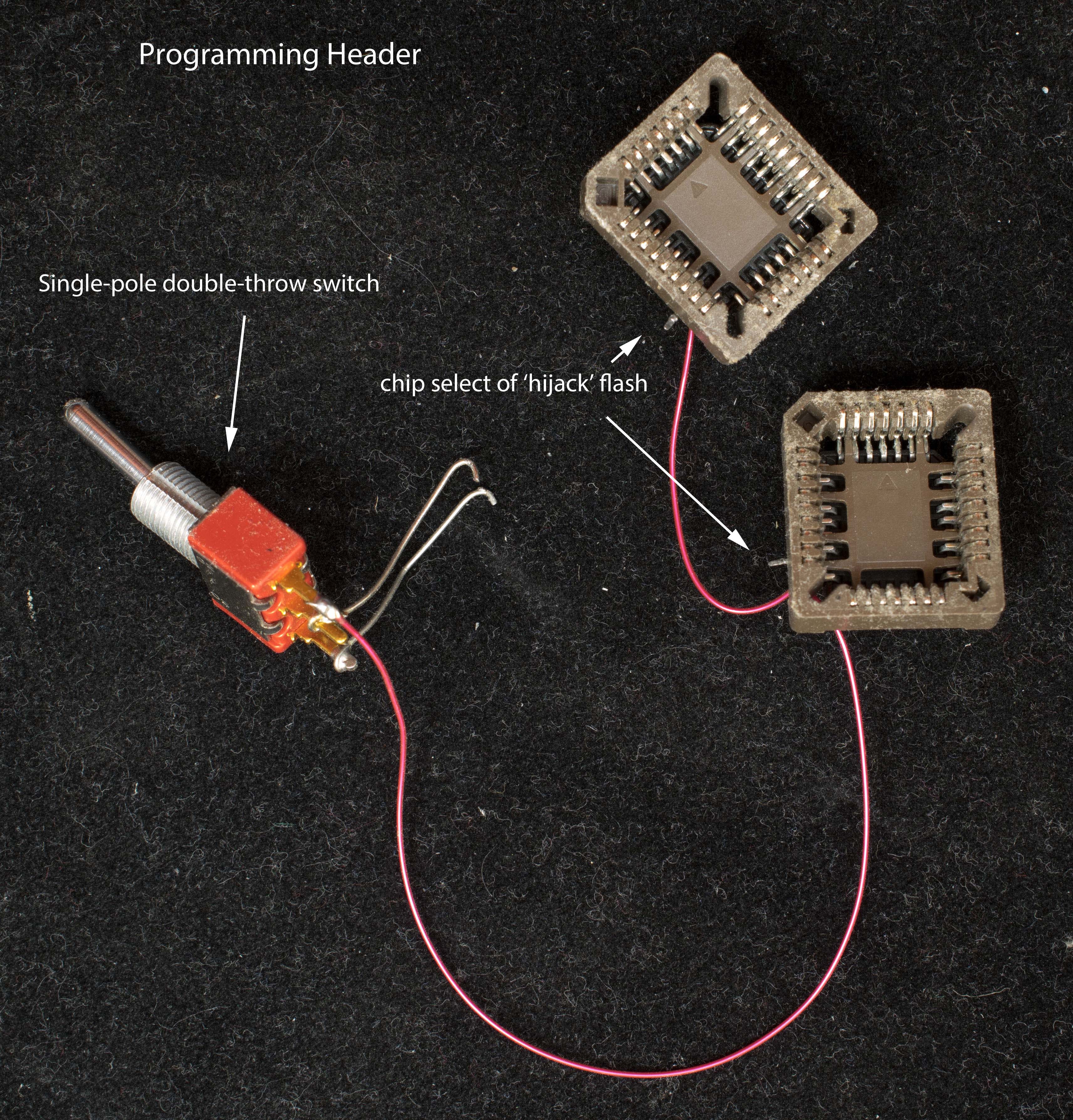
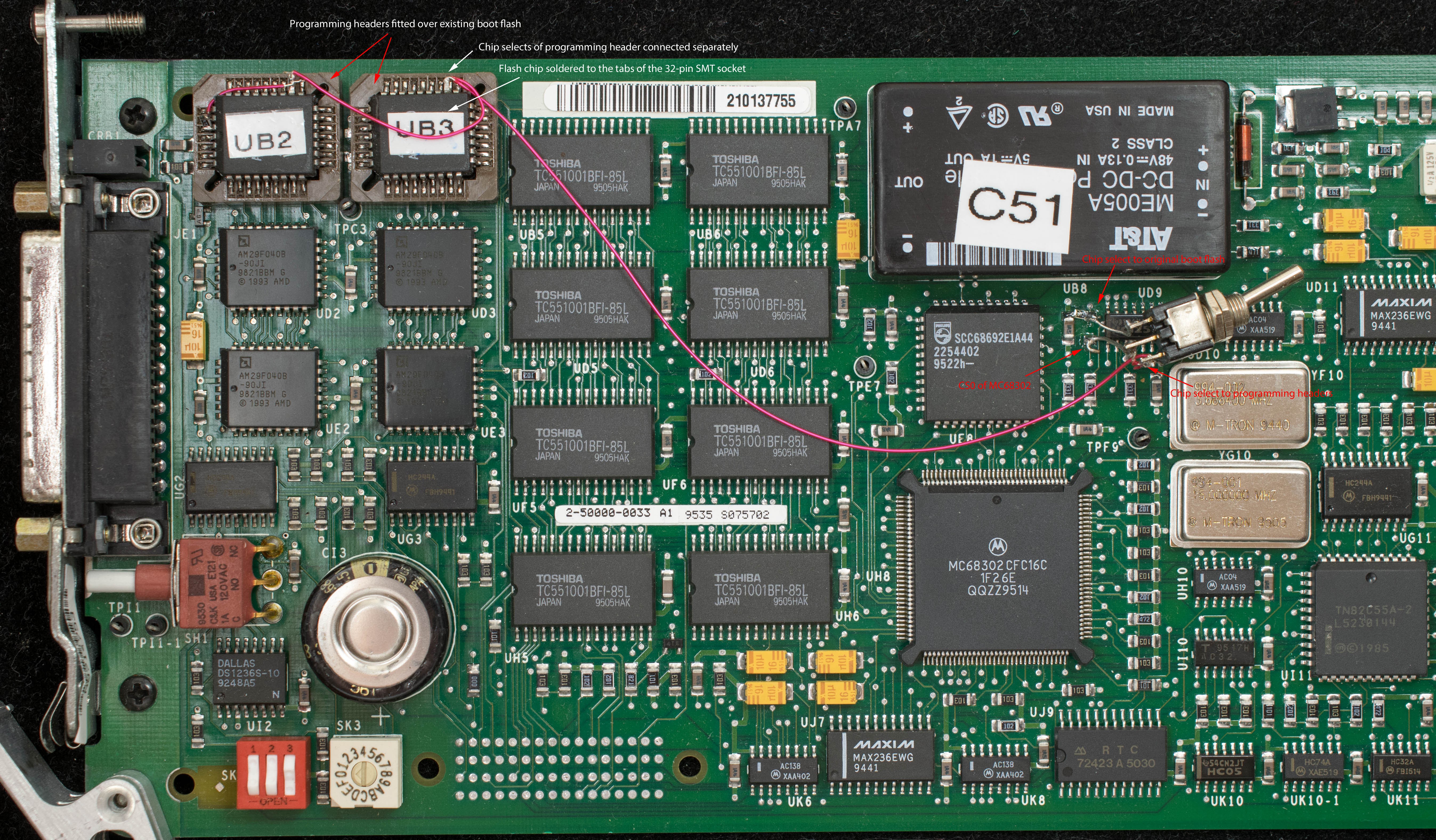
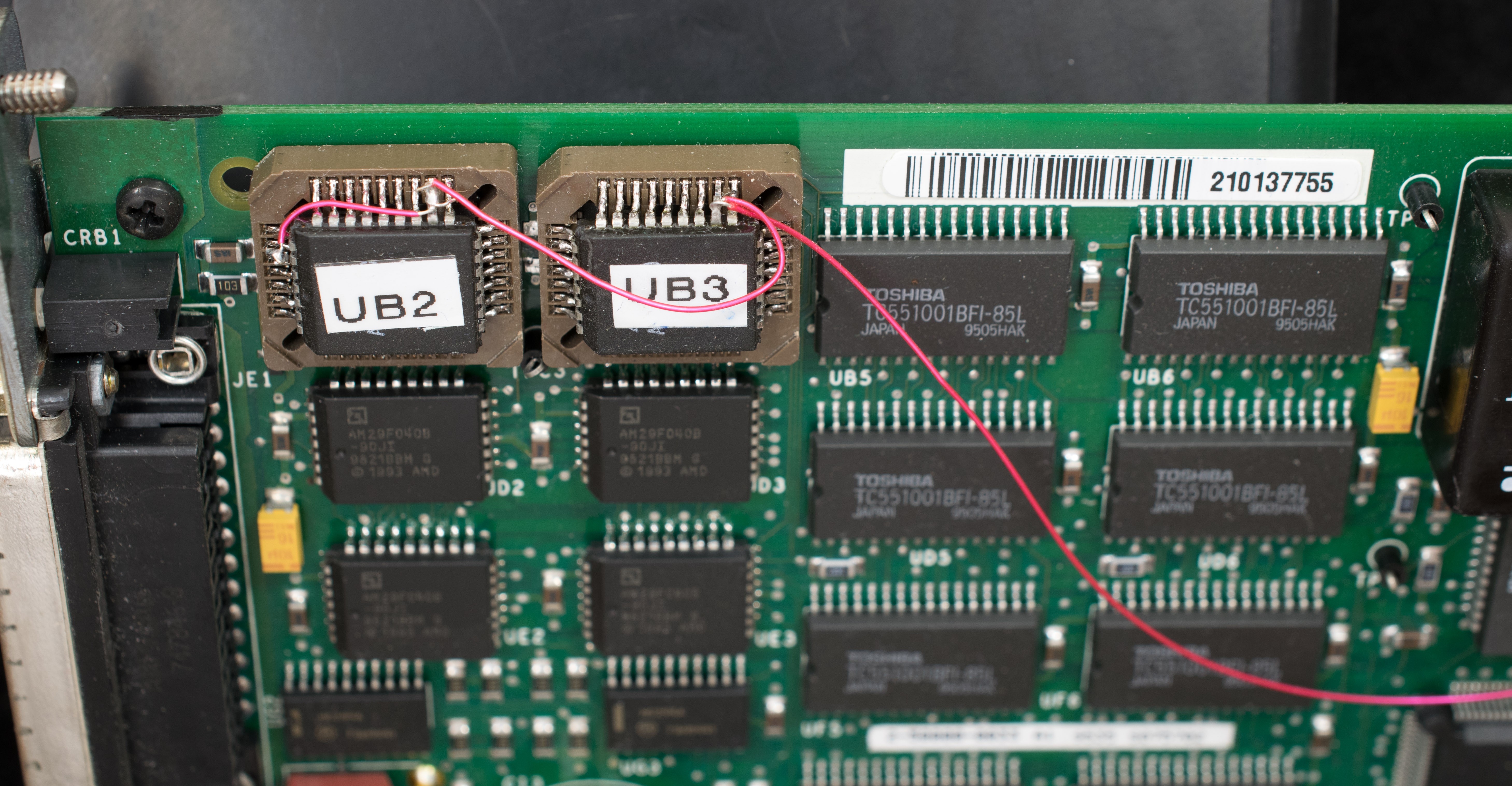
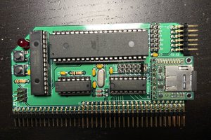
Hijacked, taking control over the original software

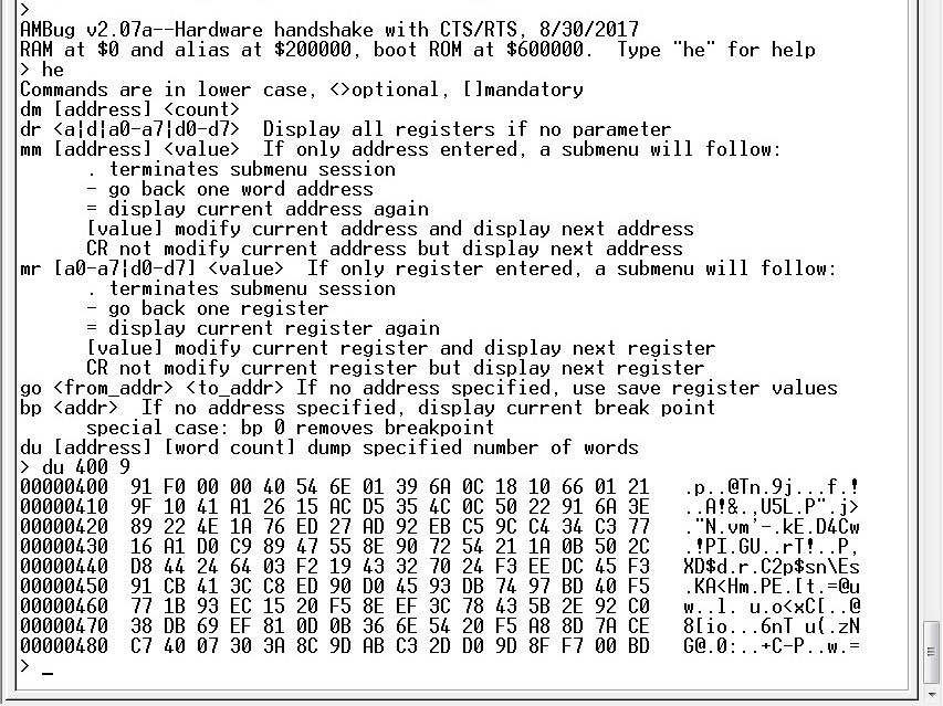
A Working Monitor/Debugger, installing my own monitor/debugger

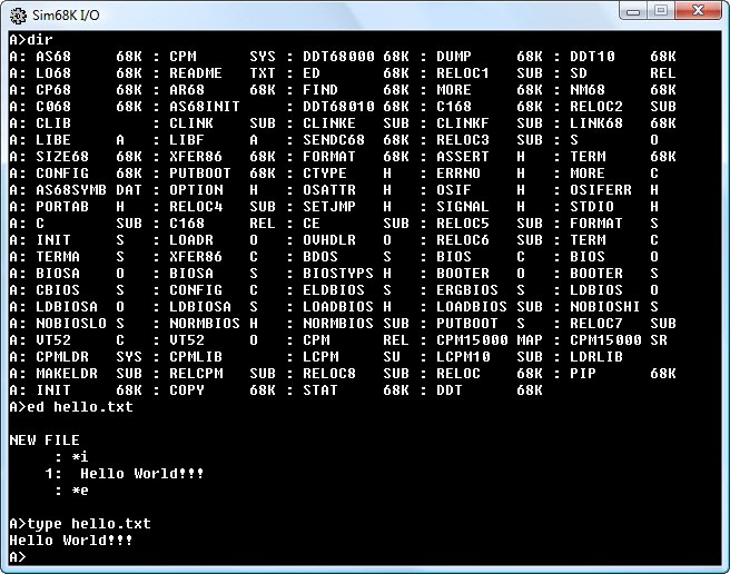
porting CP/M-68K part 1, 4-part projects on porting CP/M68K to MPU302

porting CP/M-68K part 2,

porting CP/M-68K part 3,

porting CP/M-68K part 4,

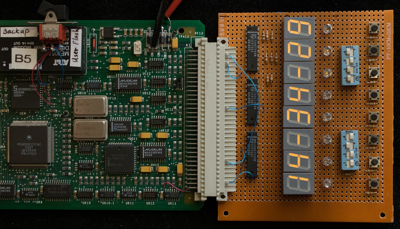
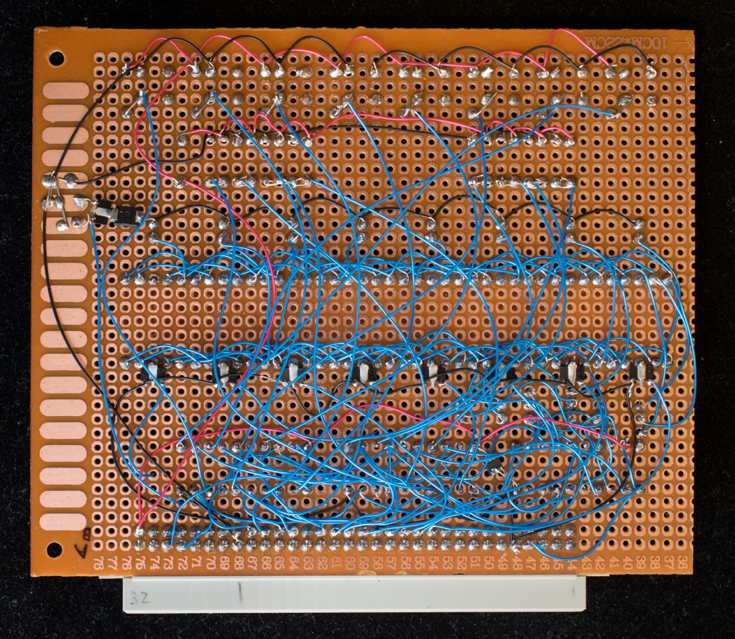
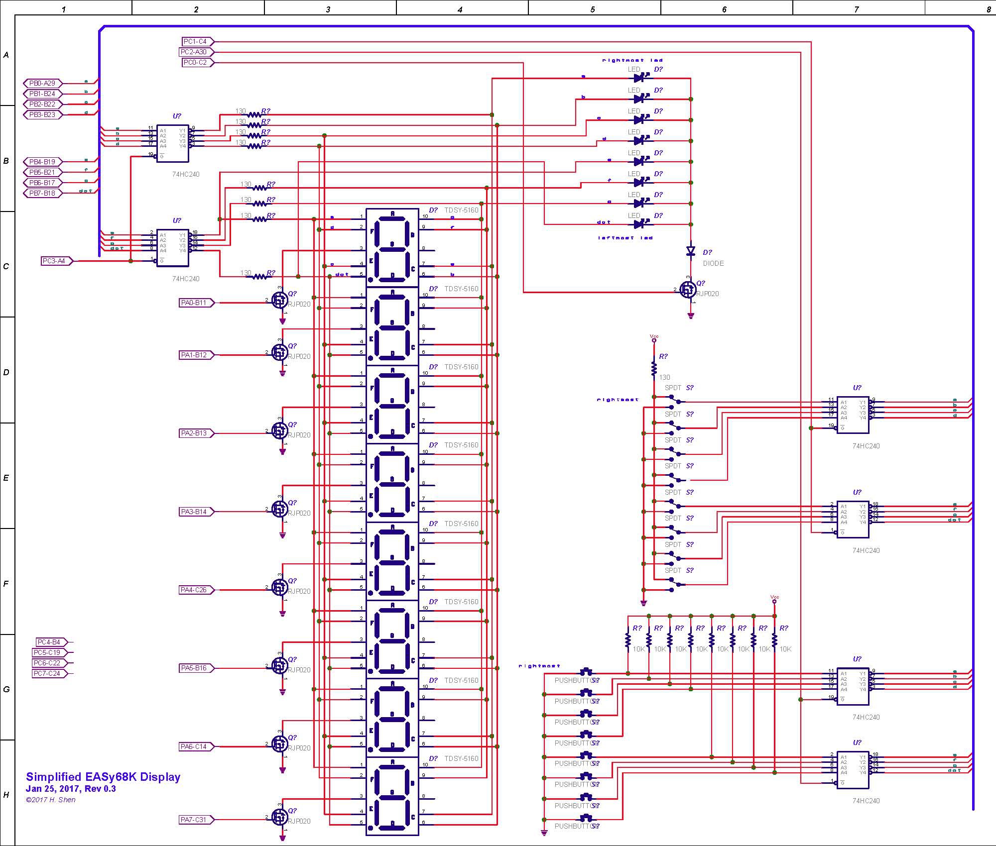
Let There Be Light, a project with MPU302, adding 7-segment display to expansion port

cpm68k_4_sim68k.zip

EASy68K simulation files. Load MPUBIOS.S68 in Sim68K first, then use the 'File'->'Open Data' submenu to load CPM15000.s68, SIMDSKA.s68, SIMDSKB.s68. Then set the PC register to 15000 and run (F9). You'll see the CP/M prompt at Sim68K I/O console.

x-zip-compressed - 1007.27 kB - 01/18/2020 at 00:08

Download

DINIDECF.zip

Gerber photo plots of CF daughterboard, rev 1. Manufactured by SeeedStudio

x-zip-compressed - 28.20 kB - 12/30/2017 at 16:03

Download

DINIDECF_scm.pdf

Schematic for CF daughterboard.

Adobe Portable Document Format - 24.64 kB - 12/30/2017 at 16:02

Preview
Download

Adobe Portable Document Format - 20.33 kB - 12/27/2017 at 15:12

Preview
Download

MPUBIOS_v2_1.zip

CP/M 68K BIOS for MPU302

x-zip-compressed - 18.72 kB - 12/26/2017 at 16:34

Download

View all 9 files

  • 1 × MC68302 Microcontroller with 68000 core
  • 2 × AM29F010 128K X 8 Flash memory
  • 4 × AM29F040 512K x 8 Flash memory
  • 8 × KM681000 128K X 8 Static RAM
  • 1 × SCC68692 Duarl UART

View all 8 components

  • Let There Be (Eco-Friendly) Light

    Plasmode01/16/2018 at 16:13 0 comments

    This is the simplified version of EASy68K compatible display.  Instead of 13 IC's, the simplified version has only 3 IC's.  It is certainly a lot easier to hand-wire!  The drawback is that it requires the microprocessor to refresh the display constantly since only one digit is displayed at any given time.  In this implementation, the display is driven by the foreground idle task when processor is not doing anything.  I kinda like that "drawback" feature because it indirectly shows the processor utilization--when the display starts to flicker, that means the processor is busily doing other works.  The power consumption is also significantly lower: it is about 150mA instead of 1 amp for the full-on 8-digit display. 

    The program running on the display is Lee Davison's 'LED clock' taken from the example page:
    http://www.easy68k.com/easy68kexamples.htm 

  • Port CP/M-68K to MPU302, part 4

    Plasmode12/30/2017 at 16:00 0 comments

    The compact flash breadboard is turned into a pc board.  I added a 2.5mm power jack for 5V power.  When plugged in, the daughterboard ground one of the discrete inputs on the DIN41612 connector.  During CP/M initialization the BIOS checks the discrete input and automatically adds the CF drives if the daughterboard is detected.  The board also bring out the 2nd serial port to a header as well as the SPI interface of 68302.  This should make experimenting with SPI & serial interface easier.  It is a very simple design and produced by SeeedStudio for 49 cents/pcs (in quantity of 10).  Shipping from China, $20, is by far the most expensive part.

    The schematic, Gerber photo plots are uploaded in the Files section.  Below is the picture of CF daughterboard plugged into a MPU302.

  • Port CP/M-68K to MPU302, part 3

    Plasmode12/27/2017 at 15:10 0 comments

    Running 68302 at 16MHz with zero wait-state memories using flash disk and RAM disk, MPU302 is a very fast CP/M machine.  The one glaring problem is the lack of mass storage.  The flash disk is write-only and the RAMdisk is only 256K byte in size.  It is fast, but not enough storage to do meaningful works.  So the next step is finding a mass storage solution.

    There is a 82C55 Programmable Peripheral Interface on the MPU302 board and all its port signals are available on the DIN 41612 connector.  That's 24 programmable I/O lines.  Compactflash interface needs 16 data lines, 3 address lines, RESET, ChipSelect, Read, and Write.  So the 82C55 can drive the compactflash interface with 1 spare line.  The software for 82C55 is not straightforward because the processor needs to poll the status of the CF register between commands and data transfers.  Switching the 82C55 from read mode to write mode or write to read causes the control port to reset to zero.  This is undesirable because CF control lines are active low so resetting the 82C55 control port will cause CF to become active.  The CF signals RESET, ChipSelect, Read, Write need to be inverted.  Another problem with 82C55 interface is the software needs to bit bang the control lines to emulate CF timing.  That's slow, unlikely to achieve megabyte/sec transfer rate.  Fortunately CP/M files are generally quite small so even a hundred kilobyte/sec of transfer rate should be adequate.

    I breadboard the design first with a scrap pc board that has an interface to a 44-pin CF adapter.  The 44-pin CF adapter is a 40-pin IDE interface plus 4 extra pins for power.  It is readily available on eBay for about $2.50.  I bought mine here: https://www.ebay.com/itm/IDE-44-Pin-Male-to-CF-Compact-Flash-Male-Adapter-Connector-DT/252403445892

    The breadboard works well.  Transfer data from flash to CF is 20-30% slower than flash to RAM (read operation), but much slower for write operation.  I created four more 8-megabyte drives on the CF (drives D: to G:).  Now I have a usable CP/M 68K machine.

  • Port CP/M-68K to MPU302, part 2

    Plasmode12/26/2017 at 15:06 0 comments

    To move from simulated environment to real hardware, the file I/O and serial I/O services used by the simulator need to be replaced with real codes in hardware.  Since the CP/M disk image is already loaded in simulation memory and CP/M file I/O services are already created in BIOS, the only real service codes that need to be created are the console input, console output and console status services.  In EASy68K simulator they are trap #15 task 5 (console input), task 6 (console output), and task 7 (console status).  In real hardware these trap calls invoke small assembly routines that interact with the 68692 Dual UART.  These trap routines become a part of the bootstrap monitor that CP/M BIOS can call.   A subtle but important point is not allowing trap #15 to be initialized when CP/M boot.  Another word, the "Set Exception Handler Address" function (function 22) need to watch out for trap #15 address and skip over it.

    At this point it is possible to test CP/M on the hardware: load CPM15000 and BIOS at location $15000 and execute.  CP/M will boot and display the prompt "A>".  A "DIR" command will either get a "no file" response or gibberish directories.  It is a good start, but not much to do because there is no disk image.

    Putting simulated disk image in flash is a little bit more complicated due to the limitation of my simple bootstrap monitor.  The disk image is located in the same address as the on-board 2 megabyte flash, but I can't write to flash directly.  I need to buffer the incoming data, erase the flash, write the data to flash one sector at a time, and verify.  That's a bit complicated for the simple bootstrap monitor.  What I've done is to cut the disk image into three parts, each part is small enough to fit in the 1 meg system RAM and have a flash programmer that copy the partial image into flash.  Once the entire disk image is reassembled in flash, load the CPM15000 and BIOS like before and execute.  Voila!

    Serially load CP/M and BIOS every time is a pain.  To speed it up, I store the CP/M and BIOS images in the flash and added a command "bo" to the bootstrap monitor.  So now I just type "bo" after power on and I'm in CP/M immediately.

  • Port CP/M-68K to MPU302, part 1

    Plasmode12/23/2017 at 18:12 0 comments

    Since the salvaged SPX-MPU board is now a general-purpose 68302 SBC unrelated to the Soneplex products, I will hereafter refer it as MPU302.

    Having 2.25 megabyte of flash and 1 megabyte of RAM, the MPU302 should be able to run CP/M-68K.  Furthermore, the top 256K of the 1 megabyte RAM is backed up with a super capacitor with a data retention period of many weeks, the top 256K RAM can serve as a RAMdisk.  Some of the remaining 768K of RAM is for monitor, CP/M, and BIOS leaving 640k for TPA.  640K, as a famous person once said, 'ought to be enough for anyone'!

    My first challenge is that I don't know much about CP/M and don't own an actual CP/M computer.  Fortunately CP/M was designed to be ported to many different hardware and good documentations are still available on the web even after 35 years.  cpm.z80.de contains a wealth of CP/M related information.  Here are links for CP/M binaries and documentation I used for my porting:

    http://cpm.z80.de/download/68kv1_3.zip CP/M 68K binaries  <- CP/M 68K ver 1.3 binaries
    http://cpm.z80.de/manuals/sys68k-m.zip System Guide  <-CP/M porting guide

    The system guide is very helpful in getting CP/M started.  The first step is to develop a BIOS specific to my hardware.  The system guide even have a BIOS template in Appendix B.  To test the BIOS, I need to have a 68000 assembler and simulator.  The SIM68K simulator of the EASy68K toolset is a very capable simulator, but there are no instruction to how to use it to simulate CP/M.  After much fumbling around and reading various CP/M porting experiences on the web, the following is my procedure for simulation CP/M68K with SIM68K:

    1.  Study the CP/M System Guide carefully, very very carefully in my case because this is all new to me.
    2.  Use cpmtools to create a CP/M disk image  (cpmtools download at http://www.moria.de/~michael/cpmtools/):

    •    Unzip the 68kv1_3.zip which resulted in 9 subdirectories containing the entire ver 1.3 distribution files.
    •   Create an entry in diskdefs with the same disk parameter block attributes as the BIOS.
    •   Create a 2-megabyte disk image with mkfs.cpm.  2 megabyte is the maximum data size that'll fit in my flash memory.
    •   Use cpmcp to copy the v1.3 distribution files into the 2-megabyte image.  This creates a disk image that has all CP/M68K distribution files in a virtual disk.
    •   The disk image is in binary format.  SIM68K expects S record datafile at the appropriate address.  I used "BIN2MOT" utility to convert the binary image to Srecord with the correct offset.  We now have a loadable CP/M disk image.

      3.  The v1.3 distribution contains a CP/M file "CPM15000.SR" which is S-record of CCP & BDOS portion of CP/M starting at location $15000.  Change the extension to .s68, it becomes the loadable CP/M image.
      4.  BIOS follows the CPM15000 which means the _ccp is at $150BC and _init is at $1B000.  Since there are no actual disk (just memory-resident disk image), the head/track/sector algorithm simplifies to calculating offsets into memory locations correspond to a particular head/track/sector value.  This makes BIOS fairly easy to write.
      5.  Putting it all together: in SIM68K load data files of the disk image, CPM15000, and BIOS.  Set PC to 0x15000 (starting address of CPM15000) and run.  You should see the A> prompt and 'dir' command will display the following.

    CP/M68K is now running in simulation! 

    Part 2 will talk about moving from simulation to the actual hardware.

  • A working monitor/debugger

    Plasmode12/18/2017 at 01:16 0 comments

    After many iterations of software development, the current version of the monitor is 2.07.  Below is a screen shot of the monitor as it logs on.  'he' command displays the commands available.  One of the command is 'du' which dumps memory content as shown.  The source code of v2.07 is uploaded into the Files section of this project.

  • Hijacked

    Plasmode12/13/2017 at 18:09 0 comments

    Returning to the problem of replacing manufacturer's boot software with my own, there are several obvious options:
    1.  remove the boot flash and replace with sockets.  Populate the sockets with my own boot flash
    2.  Pomona makes PLCC probe that clip over the flash.  They are pretty expensive and bulky.  Maybe too bulky to fit two of them side-by-side on the pc board.
    3.  Make my own PLCC probe using PLCC sockets.

    I don't want to do option 1--too much desoldering and soldering for the number of boards I have.  For cost consideration I'll try option 3 first before option 2.  I already have a board with boot flash removed and sockets installed so I'll use it to develop my 'hijack' boot software.  The purpose of this 'hijack' boot is to take over the board at power up and have a file load utility that load a program into RAM and execute.  The program executing in RAM then erases the original flash and reprograms it with my own boot software.

    What decides the expensive option 2 vs cheap option 3 is whether a PLCC socket can make reliable contacts with all pins of the original boot flash.  The contacts need not last very long, just long enough to load a program into RAM.  By process of trials & errors, I found the contacts are actually quite reliable, good for months IF I make sure no solder flux are present on the contacts.  So this is my programming header: two 'hijack' flash soldered to PLCC sockets plus a single-pole double-throw (SPDT) switch.

    To build the programming header, I first develop a working set of 'hijack' flash using the board that has boot flash in sockets.  The 'hijack' flash need to have different device code than the original boot flash (I'll explain why shortly).  Once I have a working set of 'hijack' flash, I solder them to the solder tabs of PLCC socket, taking care no flux is on the contacts of the socket.  The chip select pins of the 'hijack' flash are bent out and pulled up with a 5K resistor, so the original boot flash's chip selects are separated from the chip selects of the 'hijack' flash.  The SPDT switch selects either the chip selects of original boot flash or the chip selects of the 'hijack' flash.

    To install the programming header, I fit the PLCC socket over the corresponding original boot flash, press down firmly to make sure it makes good contact.  I remove the 330 ohm resistor between chip select 0 of 68302 and chip select of the original boot flash, solder a 5K pull up resistor to the chip select of the original boot flash and solder the remaining two terminal of the switch across the pads of the 330 ohm resistor (the common terminal to the pad leading to 68302 CS0).  With the switch set to the programming header, power up.  If the installation is done correctly, the 'hijack' flash will sign on and ready to load a program into RAM.  This program in RAM will first examine the device code of the flash.  If it is not the original boot flash, it will wait until the SPDT is switch over to the original boot flash.  Once it recognizes the device code of the original flash, it will erase the flash and copy a new boot software into the original flash.  The hijacking is complete, I am now in control of the board!

  • From PC board to schematic

    Plasmode12/12/2017 at 19:58 0 comments

    Getting schematic out of a pc board requires a little bit of luck and a lot of patience.  Luck because this is a 6-layer pc board and I'm lucky the power/ground layers are in the middle and that few boards have translucent prepreg so it is possible to see the inner layer visually.  Patience because most of the works are just tedious tracing of connections from one point to the next.  A schematic drawing program is nice to have so I can put together a schematic as I go and keep track of the signals that are not yet traced out.

    The memory subsystem is fairly easy to figure out simply because there are limited ways that memories can be connected to a processor.  It is not so much tracing but confirming connections with continuity meter.  This is fortuitous because I can write software for the board with just the knowledge of the memory subsystem.  I can then use the software to probe the rest of system.

    Figuring out the random logic connections, on the other hand, are quite tedious.  Visually tracing a connection from the component side going under a component to solder side and then verify it with a continuity meter is a very slow, tedious process.  Two methods to speed up the process:
    1.  Find a board with transparent prepreg where inner signal layers are visible and remove all components.
    2.  Take high-resolution pictures of the component side and the er side. Mirror the solder side image, align both layers in Photoshop and use the 'layer' feature of Photoshop to alternate between component side and solder side as I traced the connection.

    I worked on the schematic on and off, mostly when I need to control a portion of the logic or figure out what signals are brought out to the connectors.  I finally completed the schematic in Oct-Nov of 2017.  There are 3 sheets of schematics, memory subsystem, I/O, and reset logic.  They are posted in the 'files' section of this project.

  • Paradigm Shift

    Plasmode12/10/2017 at 17:09 0 comments

    (This is continuation of my previous log on what I've done up to a year ago.)

    My first approach was to understand how SPX-MPU handles file upload and run.  If successful, I'll be able to load and run my own software.  This is desirable because I have quite a number of these boards and I don't want to do complex hardware modifications to each one of the boards.  Unfortunately the factory software was more complex than I can handle.  The relatively simple hardware monitor tool was not adequate to follow the complex software execution.  

    I needed a different approach.   I already have a board heavily modified with hardware debugger that can load and execute programs.  So forget about working with the factory software, erase it and put my own bootstrap monitor there.  I now turned the purpose of hardware debugger around and used it as a software development platform instead.  I did not have a flash programmer for SMT components, so this debugger also served as a crude SMT flash programmer.

    I only needed a simple bootstrap that allowed me to load more sophisticated monitor and re-program itself.  Relocatable self-modifying bootstrap monitor became an essential feature of subsequent versions of the monitor.  68302 has 4 programmable chip selects, including the chip select for boot flash.  The monitor loads a small program into 68302's internal RAM and swaps the chip selects of the RAM with boot flash so RAM is now at the lowest portion of the memory while the monitor is relocated to higher memory space.  At this point a new version of monitor can be loaded into the RAM and ran to see if it is working properly.  If it checked out, the new version can overwrite the previous version.  This scheme really worked quite well.  I was able to update my monitor software numerous times without ever removing the devices.  A few times the evolving monitor had major bugs that can't communicate or reprogram itself, then I have to use the hardware debugger to load the primitive bootstrap and started over.  

    While I'm familiar with 68000, I am not familiar with the various resources on a 68302.  Furthermore I don't have schematic of the MPU board, so the monitor is the tool to explore the various resources of 68302 as well as the MPU board.  I used the wonderful tools, EASy68K, provided free by Prof Kelly at www.easy68k.com.  The simulator was useful because my 68000 assembly knowledge was rusty and I'd make rather stupid mistakes.

    At this point (beginning of 2016) I had two goals:
    1.  Reverse engineer the pc board so I have a complete schematic.
    2.  A way to reprogram the factory boot flash easily.  I don't want to build a hardware debugger for every board, nor do I want to remove the two boot flash and replace with sockets.

  • Flashback

    Plasmode12/09/2017 at 20:54 0 comments

    This entry is a recount of what I'd done with SPX-MPU board up until about a year ago.

    The SPX-MPU board has the following major components

    • MC68302 processor at 16MHz,
    • 2 ea AM29F010, 256 K bytes of flash,
    • 4 ea AM29F040, 2 mega bytes of flash,
    • 8 ea KM681000, 1 megabyte of RAM,
    • SCC68682, dual UART,
    • IS82C55,
    • RTC72423, real time clock backed with a super capacitor
    • DC-DC converter from 48V to 5V

    The first step is to find out how to power up the board.  With a 48V to 5V DC-DC converter, the power input should be 48V from the DIN 41612 connector.  Actually the power can be as low as 24V and still sufficient to power up the board.  When power is applied, the front panel LED turned red for a few seconds, then amber, and about 10-15 seconds later, it turns green.  Connecting a serial port to the DB25 connector at the front panel and fiddle around with few probable baud rates (9600 is the correct baud rate), it displayed the following sign-on message:

    Welcome to ADC: SONEPLEX Shelf Interface  Version 5.2.2
                    (C) Copyright 1998 ADC Telecommunications, Inc.

                          Enter User Name:


    This is encouraging.  The hardware likely had performed power-on self tests and passed.  Tried this on a dozen boards, and they all functioned similarly.  So I'm ready for the next level of probing.

    The on-line documentations are not very detailed.  I can't find details like schematic and software listings.  This is expected since this is a proprietary commercial board and I don't expect the manufacturer will release such details to the general public.  The on-line manual did mentioned that the username/password is hard coded as "Soneplex/Soneplex1".  With that I was able to poke around the software and see if I can find a way to upload my own software to the MPU board.  

    There is a menu for software upload, the protocol appeared to be Xmodem and it seemed to accept S-record file.  However, after numerous tries, I was unable to get my uploaded software to execute.  I speculated that uploaded software need to have correct checksum or some kind of verification scheme before it can execute.

    So a purely software reverse engineering attempt was not working, I need to probe the board and find out where is the boot flash and dumped out its content.   The boot flash is connected to chip select 0 (nCS0) which are UB2 & UB3 located at the upper left corner of the board.  I removed the boot flash and read out their contents, but it was a huge program using pSOS as its operating system.  It is unlikely I can figured out the algorithm by disassembling the code binaries.  So perhaps I should monitor the code execution and disassemble the snippet of code involved in software uploading.

    Toward that goal, I built two generations of hardware analyzer using Altera's 7128 and 7192 CPLD.  The choice of CPLD is constrained by the 5V operation of the board.  Altera 7000 series is about the most complex 5V CPLD available.  I suppose I can use a modern FPGA with the help of voltage translation buffers but that will turn this into a major project and I really don't have the time for that.  The EPM7192 is complex enough to have hardware state machine in the CPLD that can halt processor, display memory, write memory, and execute.  Developing the hardware analyzers was interesting, but in the end the manufacturer's code was still too complex for me to figure out.  I was stymied.

View all 10 project logs

Enjoy this project?

Share

Discussions

Plasmode wrote 03/12/2018 at 15:42 point

Hi,
Are you looking for a SonePlex SPX-MPU board?  I just list it on eBay, but it is the original unmodified board.  Let me know if you are interested in board modified for CP/M68K.
You also mentioned 68030 SBC.  I've designed one and it is in development stage.  I don't have one ready for sale.

  Are you sure? yes | no

hackaday wrote 03/12/2018 at 14:46 point

Do you have any boards for sale? I've checked eBay and there are currently none. I'd like a 68030 SBC and prefer not to re-invent the wheel!

  Are you sure? yes | no

Similar Projects

Does this project spark your interest?

Become a member to follow this project and never miss any updates