 Plasmode
This entry is a recount of what I'd done with SPX-MPU board up until about a year ago.
The SPX-MPU board has the following major components
- MC68302 processor at 16MHz,
- 2 ea AM29F010, 256 K bytes of flash,
- 4 ea AM29F040, 2 mega bytes of flash,
- 8 ea KM681000, 1 megabyte of RAM,
- SCC68682, dual UART,
- IS82C55,
- RTC72423, real time clock backed with a super capacitor
- DC-DC converter from 48V to 5V
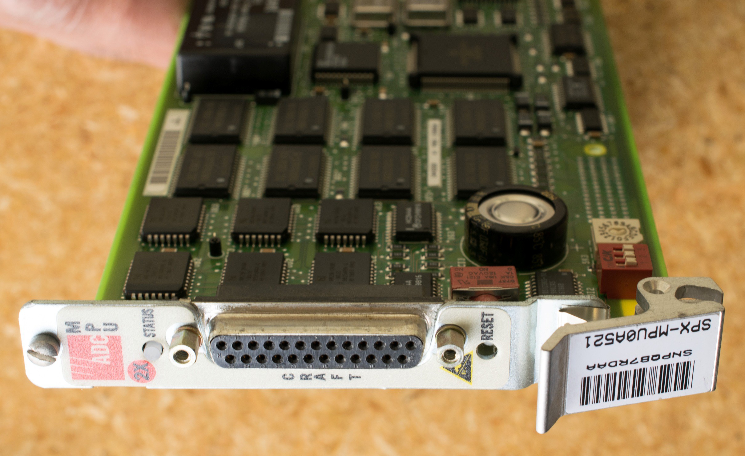
The first step is to find out how to power up the board. With a 48V to 5V DC-DC converter, the power input should be 48V from the DIN 41612 connector. Actually the power can be as low as 24V and still sufficient to power up the board. When power is applied, the front panel LED turned red for a few seconds, then amber, and about 10-15 seconds later, it turns green. Connecting a serial port to the DB25 connector at the front panel and fiddle around with few probable baud rates (9600 is the correct baud rate), it displayed the following sign-on message:
Welcome to ADC: SONEPLEX Shelf Interface Version 5.2.2
(C) Copyright 1998 ADC Telecommunications, Inc.
Enter User Name:
This is encouraging. The hardware likely had performed power-on self tests and passed. Tried this on a dozen boards, and they all functioned similarly. So I'm ready for the next level of probing.
The on-line documentations are not very detailed. I can't find details like schematic and software listings. This is expected since this is a proprietary commercial board and I don't expect the manufacturer will release such details to the general public. The on-line manual did mentioned that the username/password is hard coded as "Soneplex/Soneplex1". With that I was able to poke around the software and see if I can find a way to upload my own software to the MPU board.
There is a menu for software upload, the protocol appeared to be Xmodem and it seemed to accept S-record file. However, after numerous tries, I was unable to get my uploaded software to execute. I speculated that uploaded software need to have correct checksum or some kind of verification scheme before it can execute.
So a purely software reverse engineering attempt was not working, I need to probe the board and find out where is the boot flash and dumped out its content. The boot flash is connected to chip select 0 (nCS0) which are UB2 & UB3 located at the upper left corner of the board. I removed the boot flash and read out their contents, but it was a huge program using pSOS as its operating system. It is unlikely I can figured out the algorithm by disassembling the code binaries. So perhaps I should monitor the code execution and disassemble the snippet of code involved in software uploading.
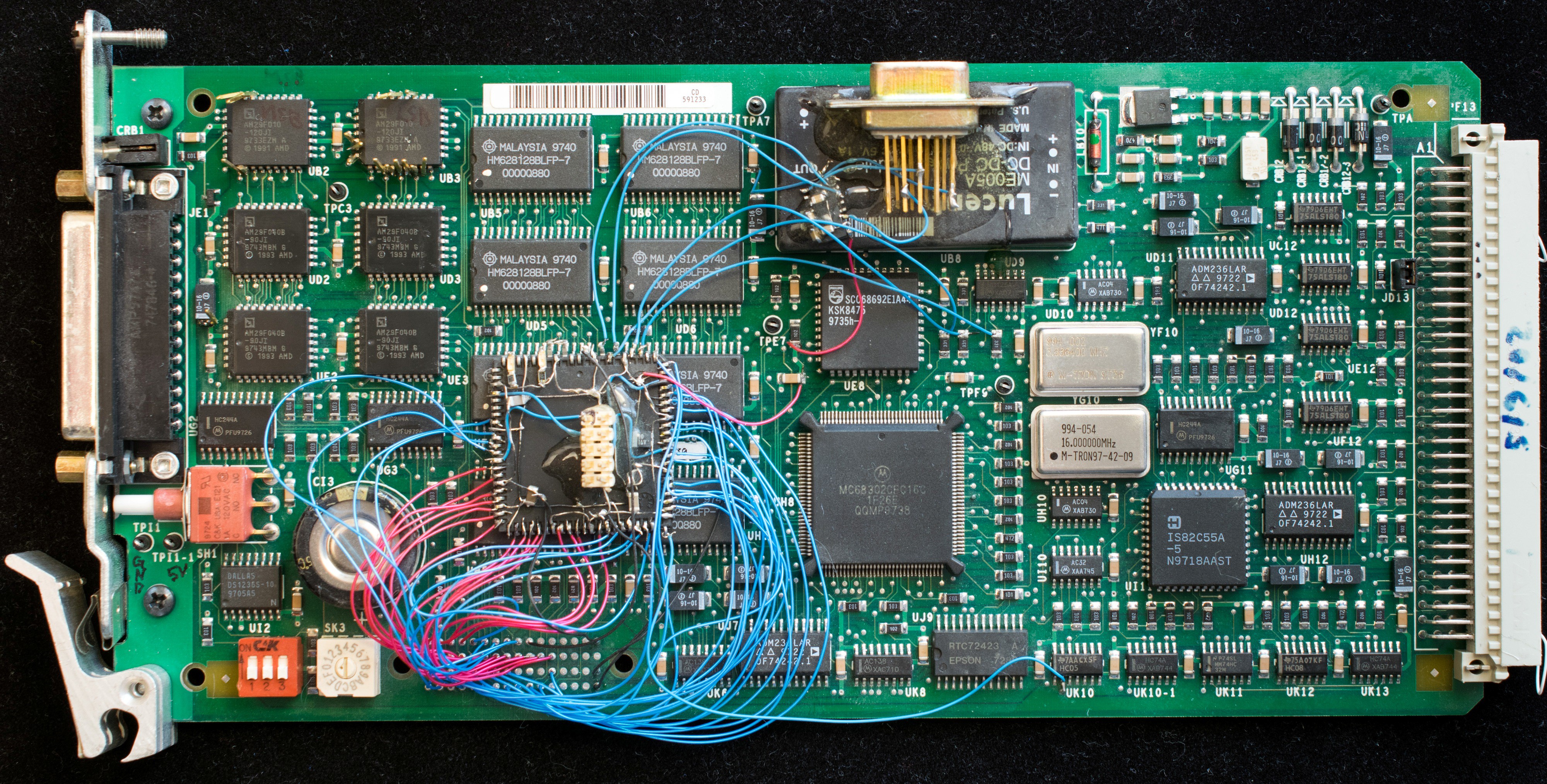
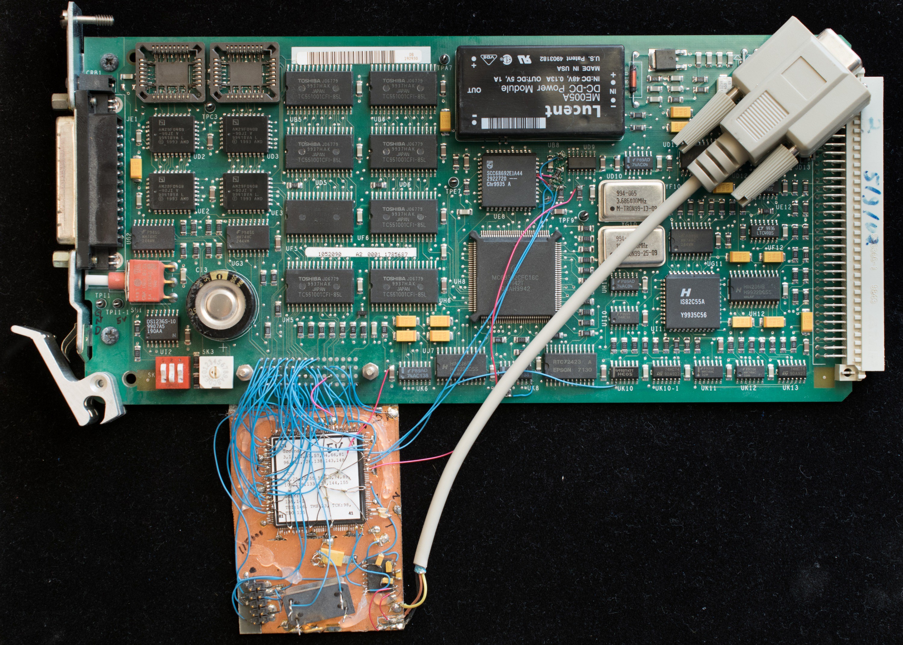
Toward that goal, I built two generations of hardware analyzer using Altera's 7128 and 7192 CPLD. The choice of CPLD is constrained by the 5V operation of the board. Altera 7000 series is about the most complex 5V CPLD available. I suppose I can use a modern FPGA with the help of voltage translation buffers but that will turn this into a major project and I really don't have the time for that. The EPM7192 is complex enough to have hardware state machine in the CPLD that can halt processor, display memory, write memory, and execute. Developing the hardware analyzers was interesting, but in the end the manufacturer's code was still too complex for me to figure out. I was stymied.
Discussions
Become a Hackaday.io Member
Create an account to leave a comment. Already have an account? Log In.