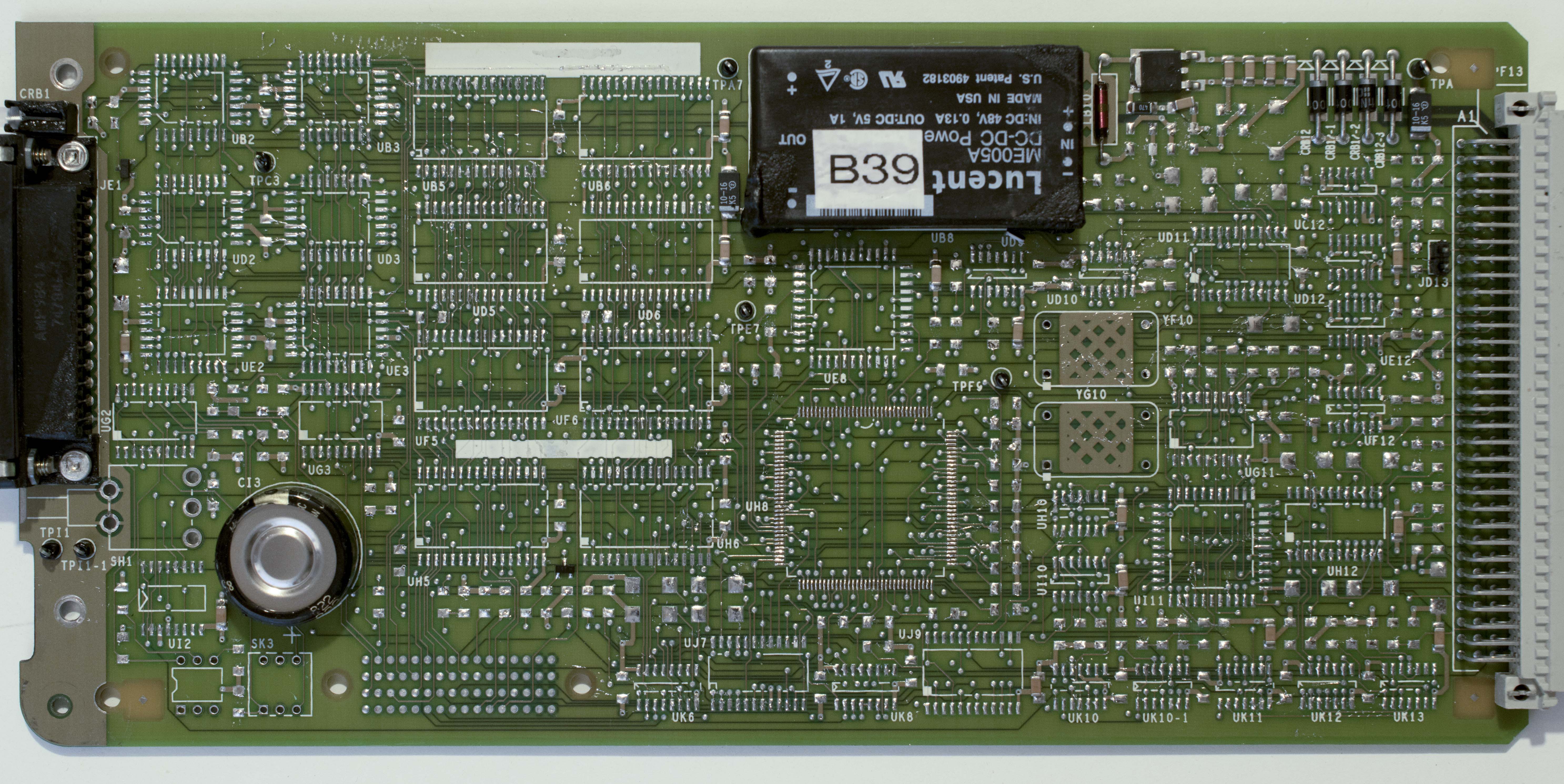
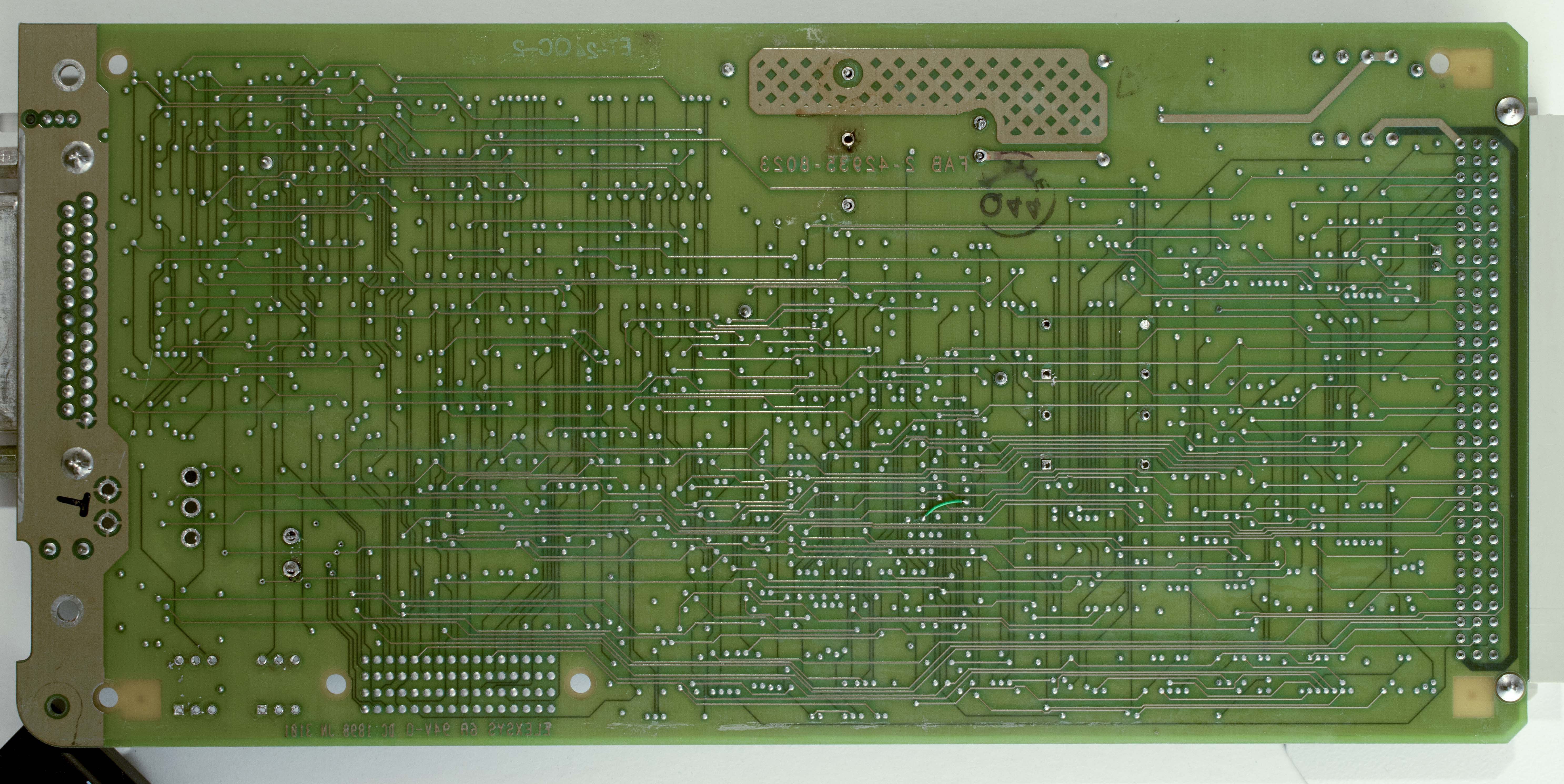
Getting schematic out of a pc board requires a little bit of luck and a lot of patience. Luck because this is a 6-layer pc board and I'm lucky the power/ground layers are in the middle and that few boards have translucent prepreg so it is possible to see the inner layer visually. Patience because most of the works are just tedious tracing of connections from one point to the next. A schematic drawing program is nice to have so I can put together a schematic as I go and keep track of the signals that are not yet traced out.
The memory subsystem is fairly easy to figure out simply because there are limited ways that memories can be connected to a processor. It is not so much tracing but confirming connections with continuity meter. This is fortuitous because I can write software for the board with just the knowledge of the memory subsystem. I can then use the software to probe the rest of system.
Figuring out the random logic connections, on the other hand, are quite tedious. Visually tracing a connection from the component side going under a component to solder side and then verify it with a continuity meter is a very slow, tedious process. Two methods to speed up the process:
1. Find a board with transparent prepreg where inner signal layers are visible and remove all components.
2. Take high-resolution pictures of the component side and the er side. Mirror the solder side image, align both layers in Photoshop and use the 'layer' feature of Photoshop to alternate between component side and solder side as I traced the connection.


I worked on the schematic on and off, mostly when I need to control a portion of the logic or figure out what signals are brought out to the connectors. I finally completed the schematic in Oct-Nov of 2017. There are 3 sheets of schematics, memory subsystem, I/O, and reset logic. They are posted in the 'files' section of this project.
 Plasmode
Discussions
Become a Hackaday.io Member
Create an account to leave a comment. Already have an account? Log In.