 Christoph Tack
Who needs this?
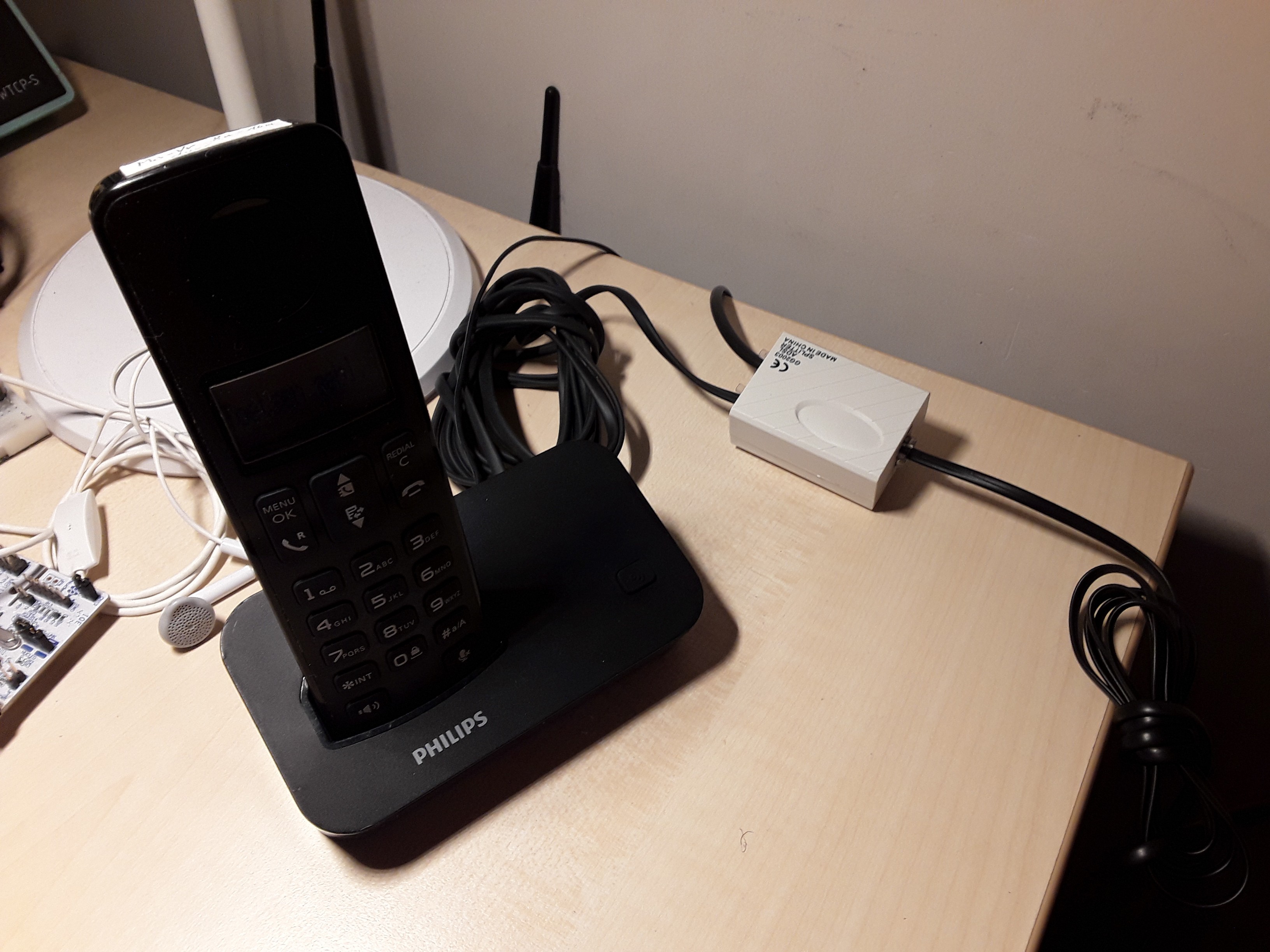
You want to use a pulse dialing telephone, but your SLIC (such as a VOIP-interface) doesn't support pulse dialing. Instead of building the project described here, you could make things easy for yourself by replacing your SLIC by one that supports pulse dialing, e.g. the Grandstream HT801 (untested) or others.
Description
Has this kind of thing been done already? Oh yes, many times. But this device will be cheaper to build and solve some shortcomings of the converters around today by being:
- insensitive to line polarity
- open source
- readily available & cheap parts (no bulky audio transformer needed)
- plug and play immediately, no 15mins pre-charging time needed
- doesn't steal power from the telephone line when the telephone horn is on-hook
- no modifications to rotary phone required
Sources
There's little more annoying on Hackaday.io than people "sharing" their project, but keeping the source files to themselves. So here you go:
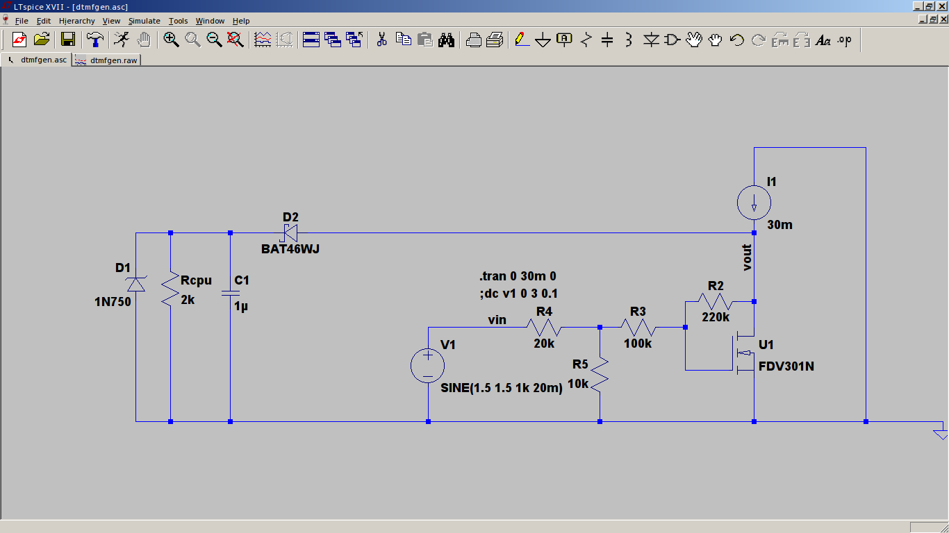
- Firmware source code can be found on : GitHub.
- Production data (hex-files, gerber files, schematics, ...) can be found on : GitHub project's releases
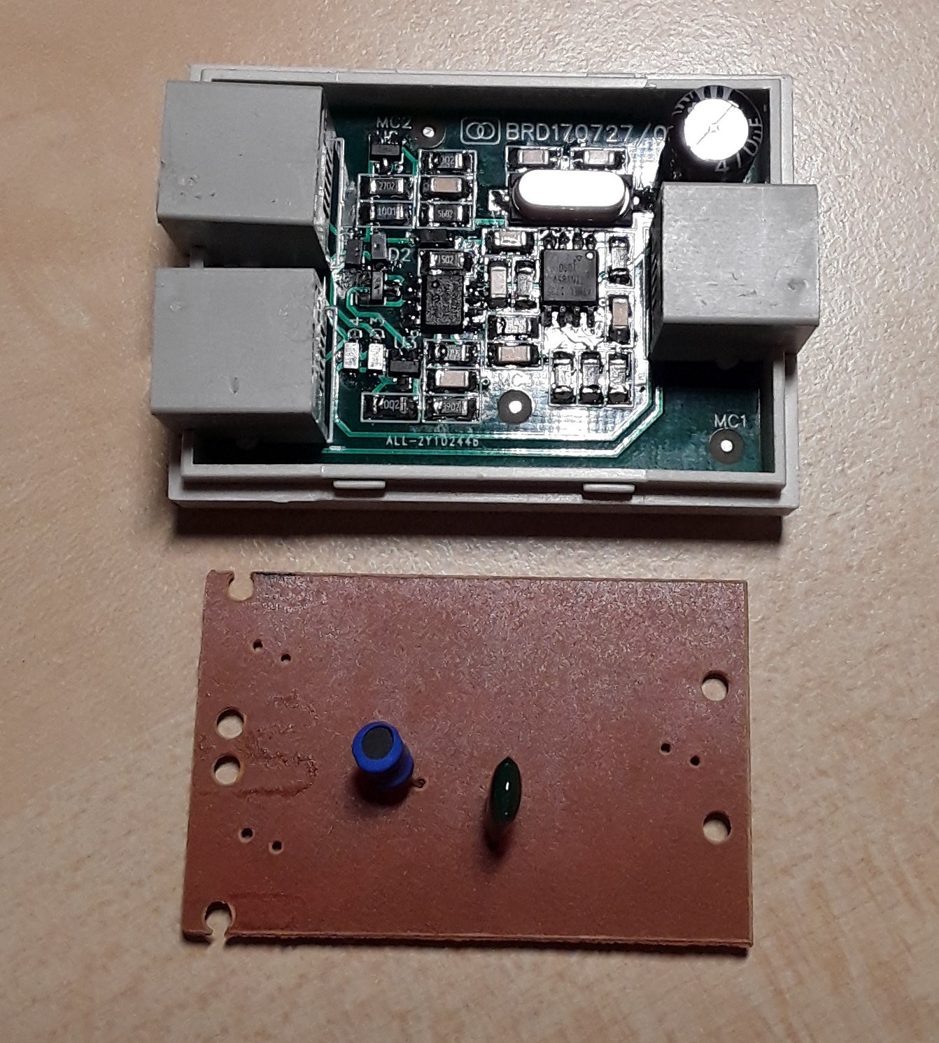
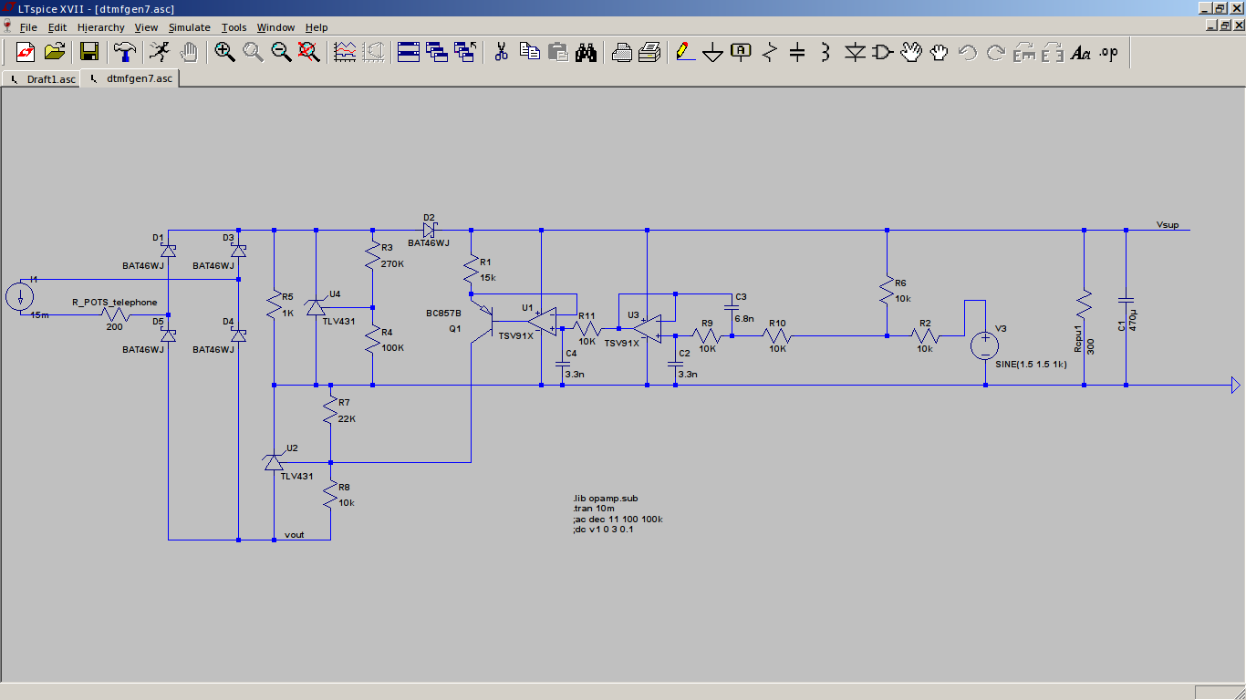
- PCB design files are online on EasyEda. The PCB design files have also been exported to Altium format and have been added to the repository on GitHub. The contents of these Altium files has not been checked.
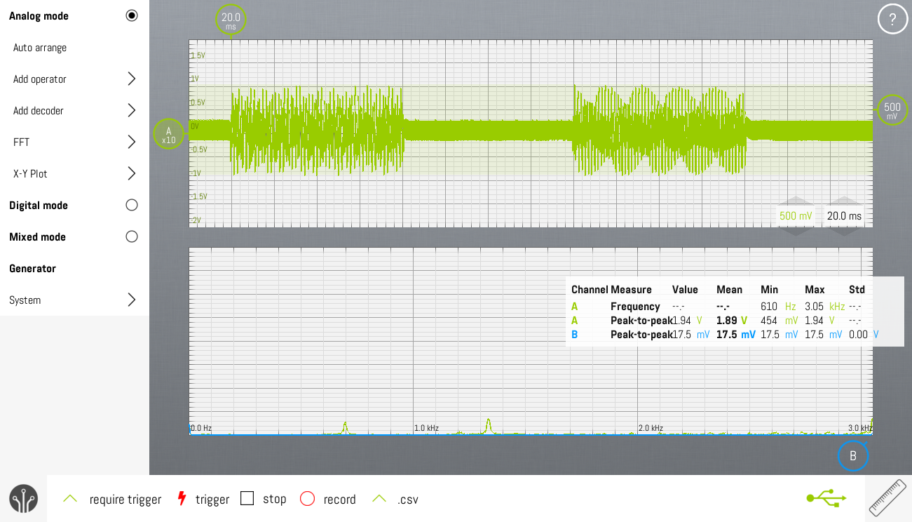
DTMF-generator standard
ETSI ES 201 235-2 V1.1.1 (2000-09) describes some rules DTMF-generators should comply to.
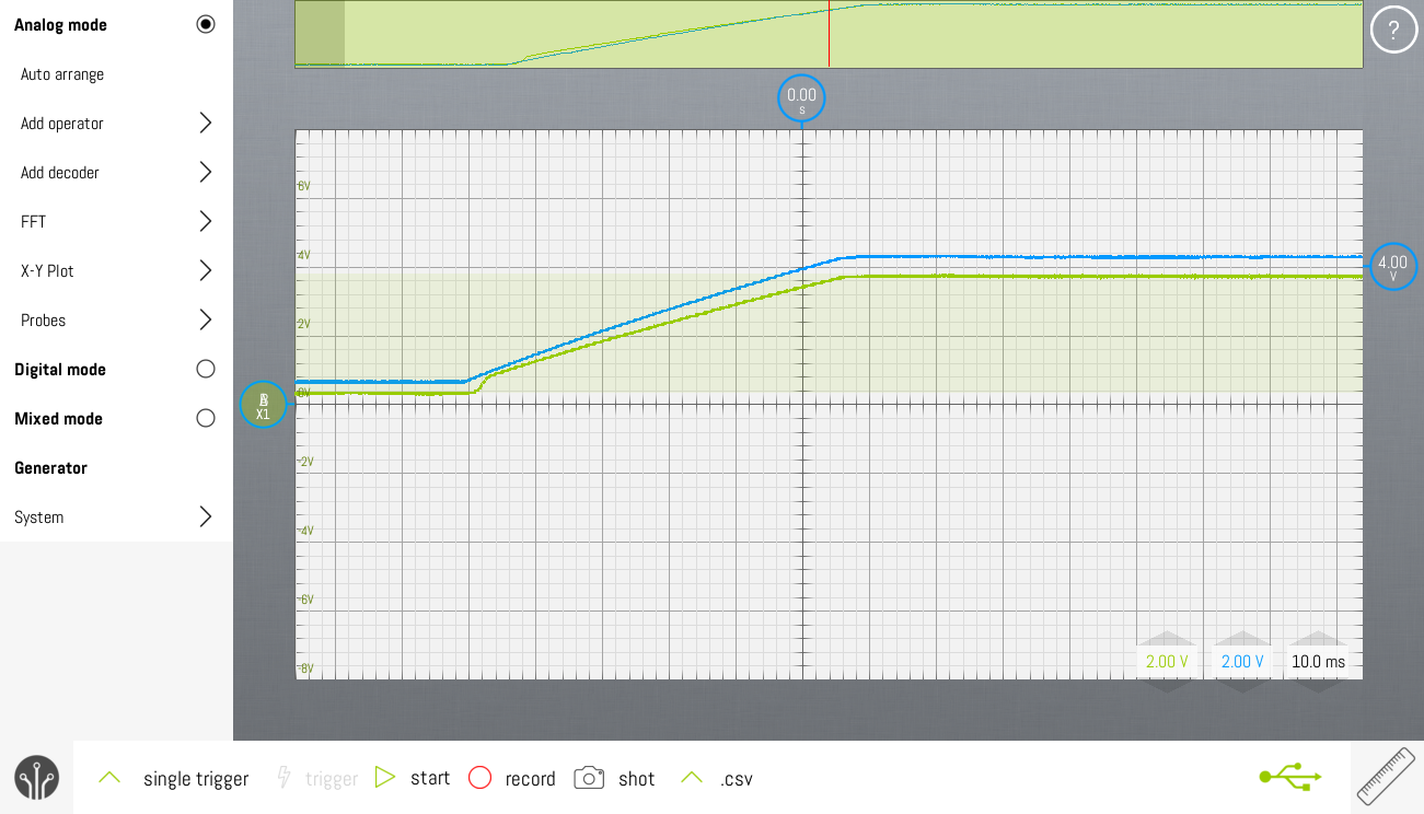
- Maximum signal amplitude : HF + LF = (-9,0 dBV, +2,0 dB) + (-11,0 dBV, +2,5 dB) = -7dBV + -8dBV = 1.26Vpp + 1.13Vpp = 2.39Vpp. Practical signal amplitudes will be much lower.
- Tone duration : 65-90ms
- Pause duration : > 65ms
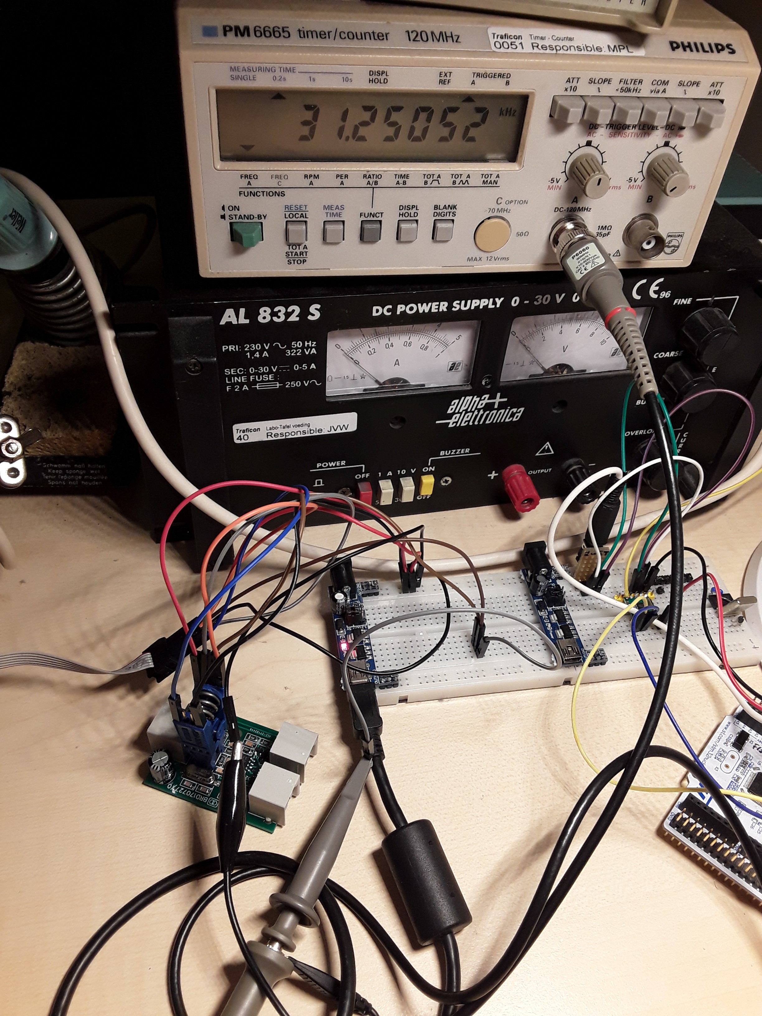
- Frequency tolerance : +/-1.5%. This implies using an external oscillator or crystal because the internal RC-oscillator is too dependent on power supply voltage and temperature.
References
Pulse to tone converters that require modifications inside the telephone:
- Boris Cherkasskiy : Rotary Dial for digital age
- Frits Kieftenbelt : T65, W65, Ericsson en Heemaf telefoon genereert DTMF tonen (dutch language)
- Anton Meyer : ArduinoDTMF
![]()
Anonymous circuit, showing how to feed your circuitry from a zener in series with the telephone line.


 Evangelos Petrongonas
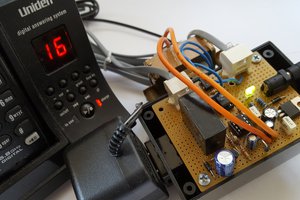
 Boelens, Leland
 Lukas Koch aka Ast
 Paul Andrews
Hello, I would like to better understand your explanation and how it works, if I buy a pcb with the files provided on your github:
1 - will there already be ports to connect cables on the motherboard or is it something to add in addition (by buying it somewhere or I'm not sure)
2 - is it plug and play, or is there a firmware to be added?
Thanks in advance
PS: if there are any mistakes in the message, it's because I'm French and I do my best with English.