0%
0%
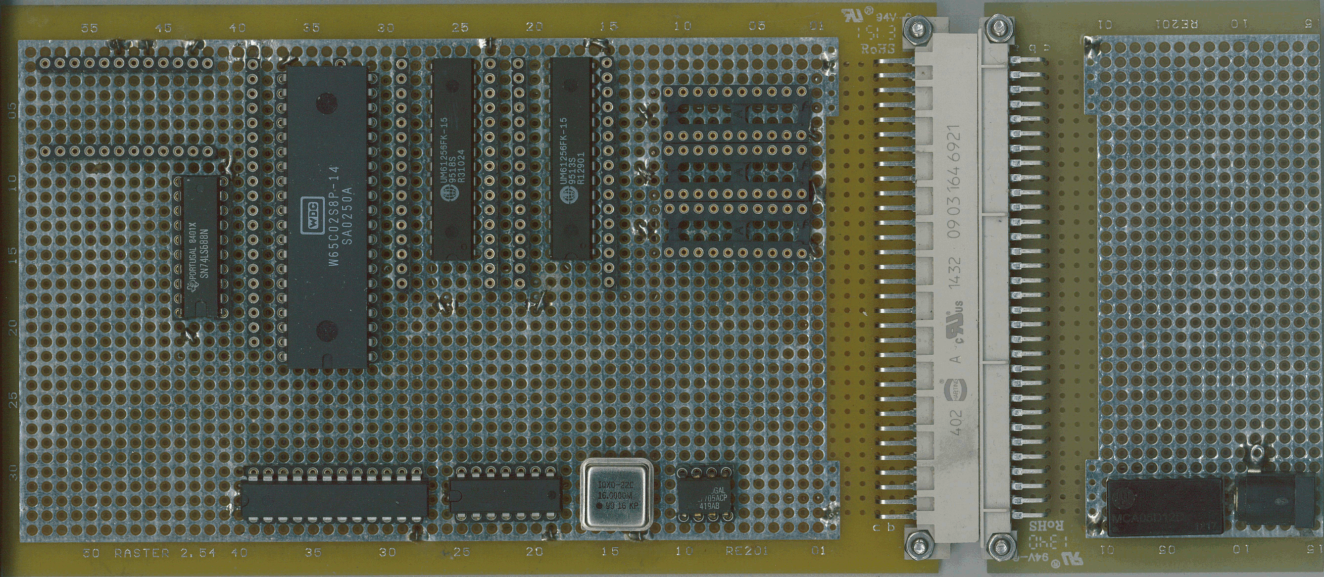
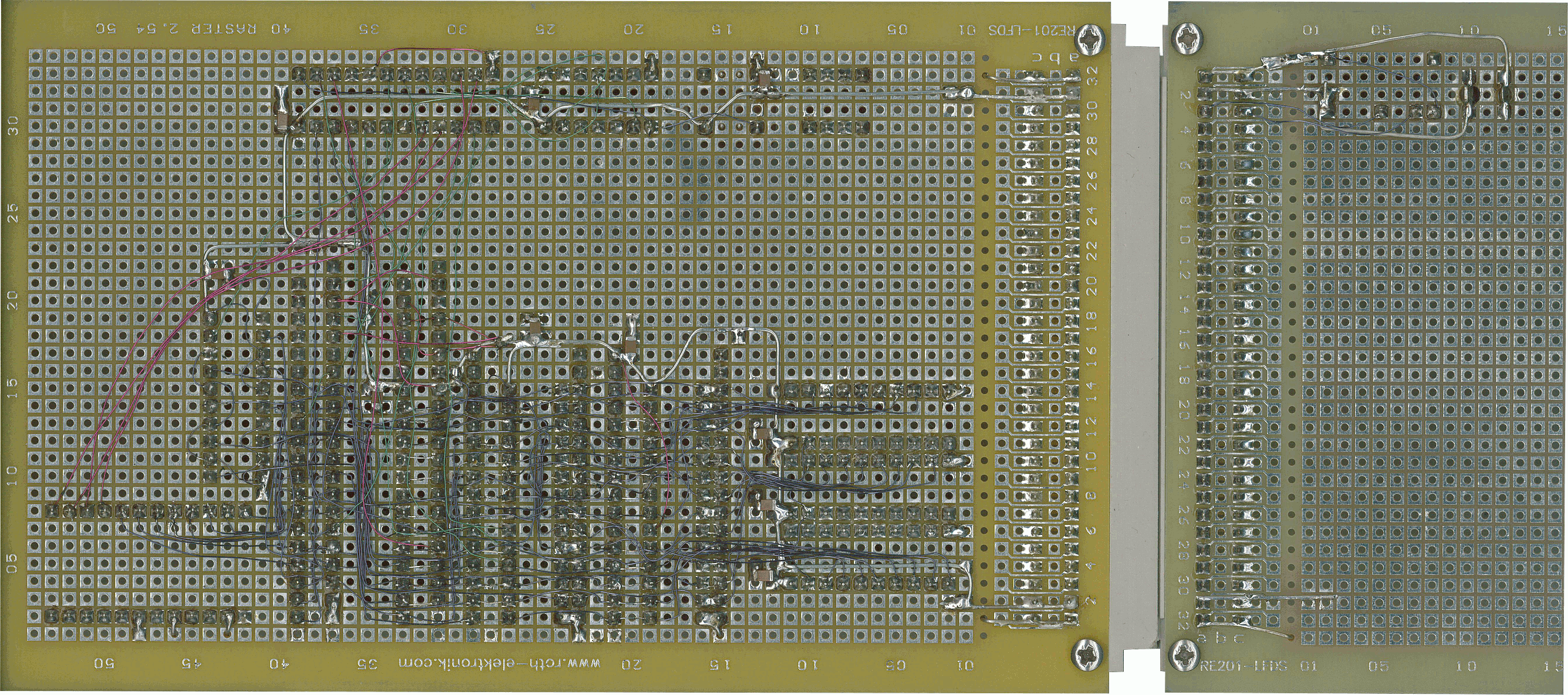
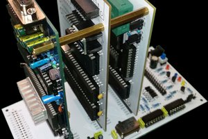
STEbus 65C02
65C02, 32K Flash ROM, 64K fast RAM, USB link to PC.
Runs BBC BASIC, at up to 14MHz.
 Keith
KeithBecome a Hackaday.io member
Already have an account? Log in.
Just one more thing
To make the experience fit your profile, pick a username and tell us what interests you.
Pick an awesome username
hackaday.io/
Your profile's URL: hackaday.io/username. Max 25 alphanumeric characters.
Pick a few interests
Projects that share your interests
People that share your interests


 Dawid Buchwald
 padnest
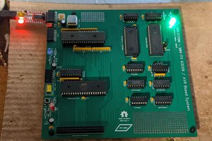
 Dave Collins
I like how this looks - is there a source for the eurocard-friendly PCB in the US?
I already have about 50 of the appropriate connectors and a P2 backplane.