 bveina
Up till now I've been prototyping with individual 5050 apa102 leds, and to wire them up I've co-opted some soic8 to dip8 breakout boards. that is not going to work in the long term. also as a contigency plan, if i run short on time id like a way to throw the leds into a quick laser cut 'form' and use that as part of the final piece, it will be messier, but i can hide any wires as needed, so i set about to create some easy to use apa102 breakout boards, cheaply.
i always try to make my own footprints before trusting anything i find in eagle. 95% of the time, everything works if you use stock components, but Murphy's Law makes that 5% of the time happen every time... so off to the data sheet. Aliexpress had some mechanical drawings on it:
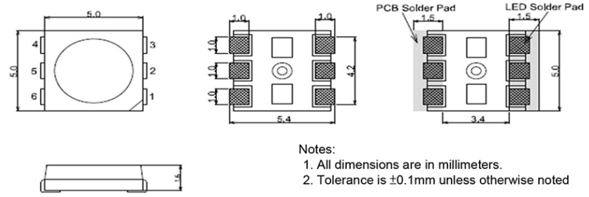
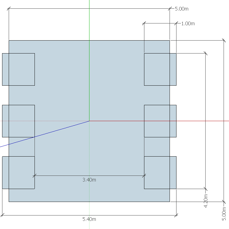
ok the componenet has 1mm x 1mm contacts, then there is 4.2mm outside to outside dimensions so the center Y value would be: divide by 3 and.. no (4.3mm-3*1mm) /3 +.. <opens Skectchup> <30 seconds later>
ok now i know where every pad is. i just need to know the recomended pcb footprint. and thats where i cant follow this datasheet, it indicates 1.5mm wide, but not where is should start nor how tall it should be. doing a quick internet search for "apa102 datasheet" yields plenty of datahsheet but not much more. "apa102 footprint" or "apa102 land pattern" dont help much more. so lacking anything more substantial ill settle for any 6 pin 5050 led.
"5050 led land pattern" on image search hits paydirt.
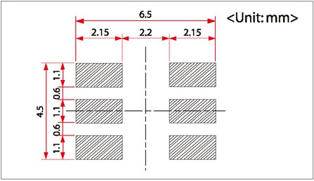
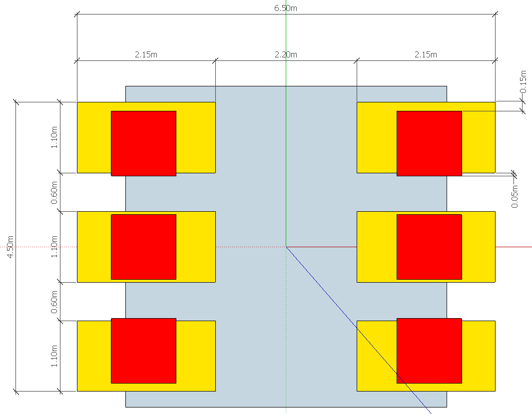
will this work with my APA102s? lets just remake this in sketchup too.
And it was at that point im reminded of a recent hackaday article "terrible dimensioned drawings" but that being said, im going to use it anyway. the error shown is 0.15mm and all the dimesions listed for the led contacts are +/- 0.1mm. like homer said "close enough."
onto eagle, very basic.
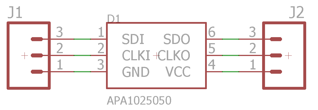
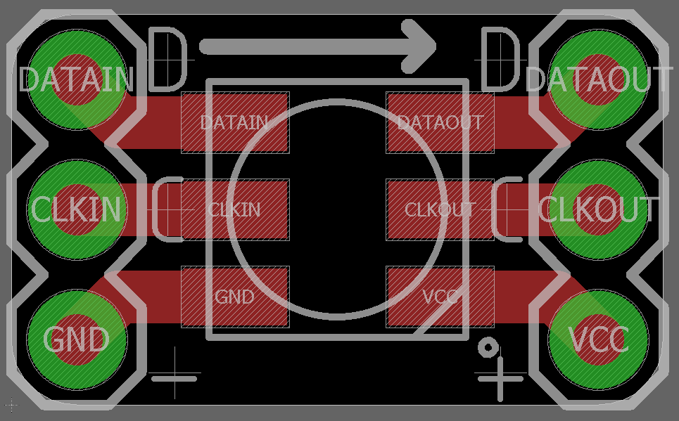 | 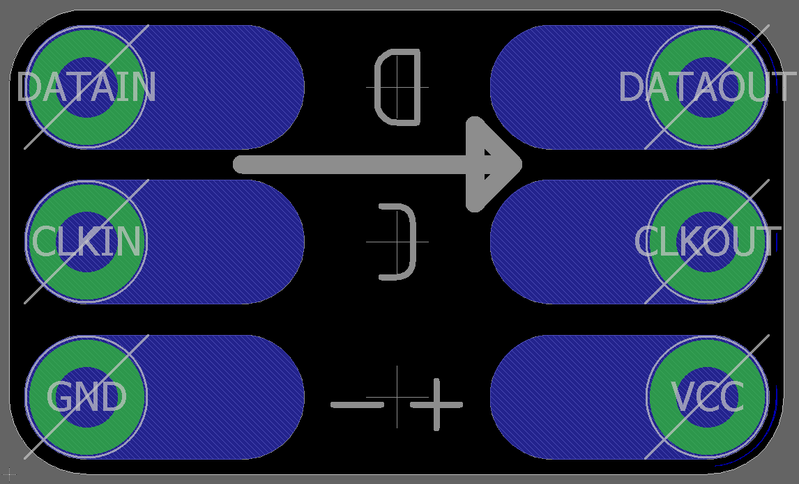 |
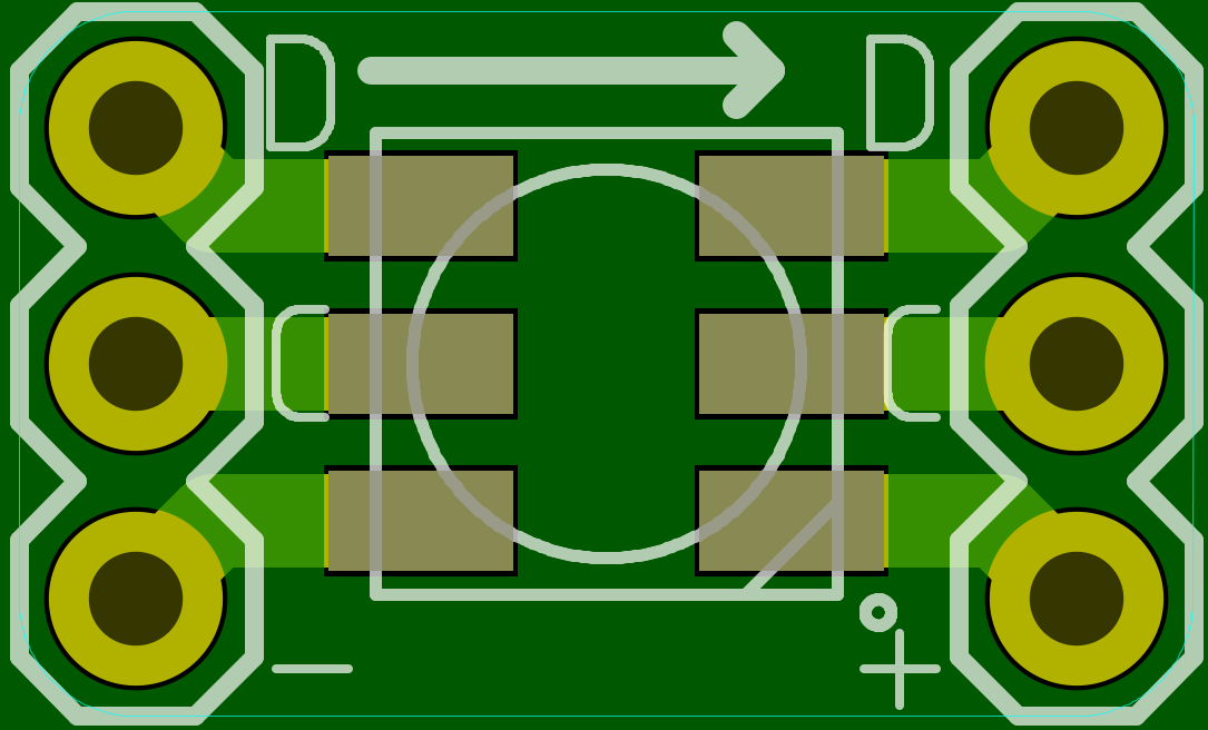 | 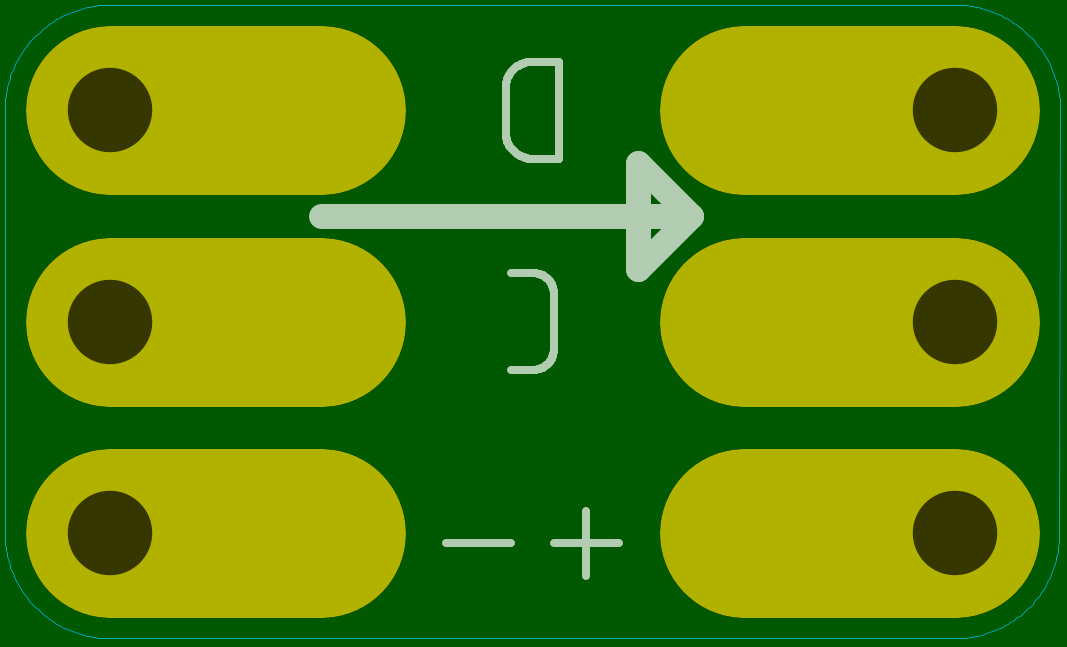 |
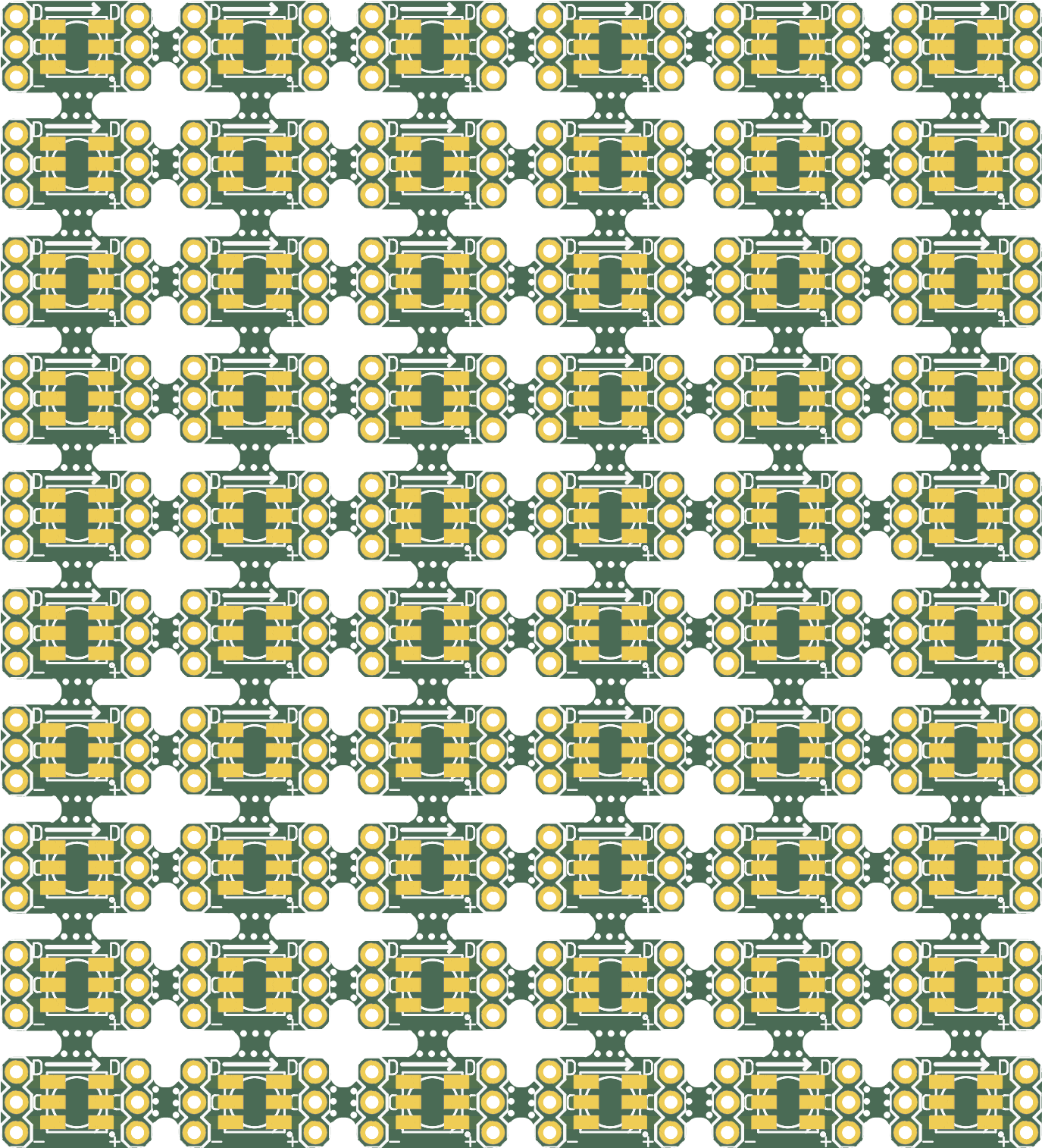
the only hacky thing i dis here was add giant traces on the bottom so i could solder wires invisibly and chain multiple wires together the bStop layer will stop soldermask from being put down. after checking the gerbers in gerbv, i set about to panelize the boards.
and, since i did something beyond just running ThisIsNotRocketScience's Gerber Panelizer ill stop this post here.
preview of next time:
Discussions
Become a Hackaday.io Member
Create an account to leave a comment. Already have an account? Log In.