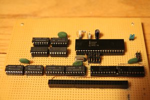
Close
0%
0%

STEbus I/O prototyping board

STEbus I/O slaves are much easier to make than masters.
This board uses simple TTL only.

Similar projects worth following
Occupies 16 i/o address locations in a 4k i/o space. Simple to use to develop your own applications.

The circuit shows how simple it is.

Technology has progressed so much that one can easily fit a megabyte of RAM on a processor board for less than the cost of a DIN41612 connector. Graphics cards are memory mapped, but these days most people have a PC they can use as a terminal, so video output is not that useful.

Many STEbus boards were designed so it is difficult to think of ones that have not already been invented. Being an industrial bus, most boards were very practical. Serial, parallel, battery-backed memory, flash memory, ADCs, DACs, data storage. 

So I try to think of things that are more frivolous and fun. Sound effects for instance. I'd like to make a sound board with the SID, AY38910, POKEY, playing music while an SP-0256 speech synthesis chip sings Benny Benassi's 'Satisfaction'. It sounds like Stephen Hawking providing backing vocals for this power tool advert:


If you really want to be nerdy, you could feed the audio into your tesla coil sound system:

If anyone can think of a better application, let me know and I will add it to the list here.

A quick google revealed that Hawking's voice is based on an ISA bus board carrying an 80188 that breaks English text into phonemes and sends them to an NEC 77P20 DSP. A lot more sophisticated than the SP-0256. Alas it is not available for download, since the original software is under copyright.

J061_cct.png

Circuit diagram

Portable Network Graphics (PNG) - 37.00 kB - 04/12/2022 at 00:47

Preview
Download

STEbus_io_prototyping_board_manual_htm.zip

How to use the I/O prototyping board.

Zip Archive - 1.31 MB - 01/08/2018 at 02:47

Download

  • Timing explained

    Keith02/26/2022 at 03:18 0 comments

    The STEbus was defined in the early 1980s, when a typical bus cycle for a processor and its support chips was about 1 microsecond. A 4 MHz Z80 took 3 or 4 clock ticks, and 8 MHz 68000 took 8 clock ticks. Memory chip speeds were about 300 to 450 ns, so not much point having a processor faster than the memory or peripherals.

    The STEbus is asynchronous - slave boards make the master wait until a bus transfer is complete and acknowledged. The data strobe is effectively delayed before returning as the acknowledge signal.

    A shift register is a way to have well-controlled delays. The diagram below shows how a logic high ripples through a 74LS164 shift register (signals QA to QH) and produce the DATACK signal when desired.

    As a bonus, they can be used to generate any timing pulse with a single AND gate and a NOT gate.

    A common example is a write pulse that must start some time after the data is valid and end some time before the data goes invalid. The lower half of the diagram shows such signals. The short one is made by ANDing QB with NOT QD.

    It is possible to create more complex signals with a little more logic. Such as signals that mimic those of  a particular peripheral chip's processor family.

View project log

Enjoy this project?

Share

Discussions

Ralphw wrote 01/04/2023 at 18:27 point

Is there a gerber file available for this board? 

I need to make a few for experiments.

  Are you sure? yes | no

Keith wrote 01/05/2023 at 19:14 point

It was laid out as red and green tape on mylar film, which is in landfill somewhere. :-(If you would like to do a remake I would be happy to help, as it is something I wanted to do myself. A later version of this board had links for the ATNREQ* lines. I would want to improve the design by making all the prototyping holes on the same grid as the DIN41612 connector. And maybe add a ground plane to allow higher speed slaves.

  Are you sure? yes | no

Similar Projects

Does this project spark your interest?

Become a member to follow this project and never miss any updates