 Keith
KeithThe STEbus was defined in the early 1980s, when a typical bus cycle for a processor and its support chips was about 1 microsecond. A 4 MHz Z80 took 3 or 4 clock ticks, and 8 MHz 68000 took 8 clock ticks. Memory chip speeds were about 300 to 450 ns, so not much point having a processor faster than the memory or peripherals.
The STEbus is asynchronous - slave boards make the master wait until a bus transfer is complete and acknowledged. The data strobe is effectively delayed before returning as the acknowledge signal.
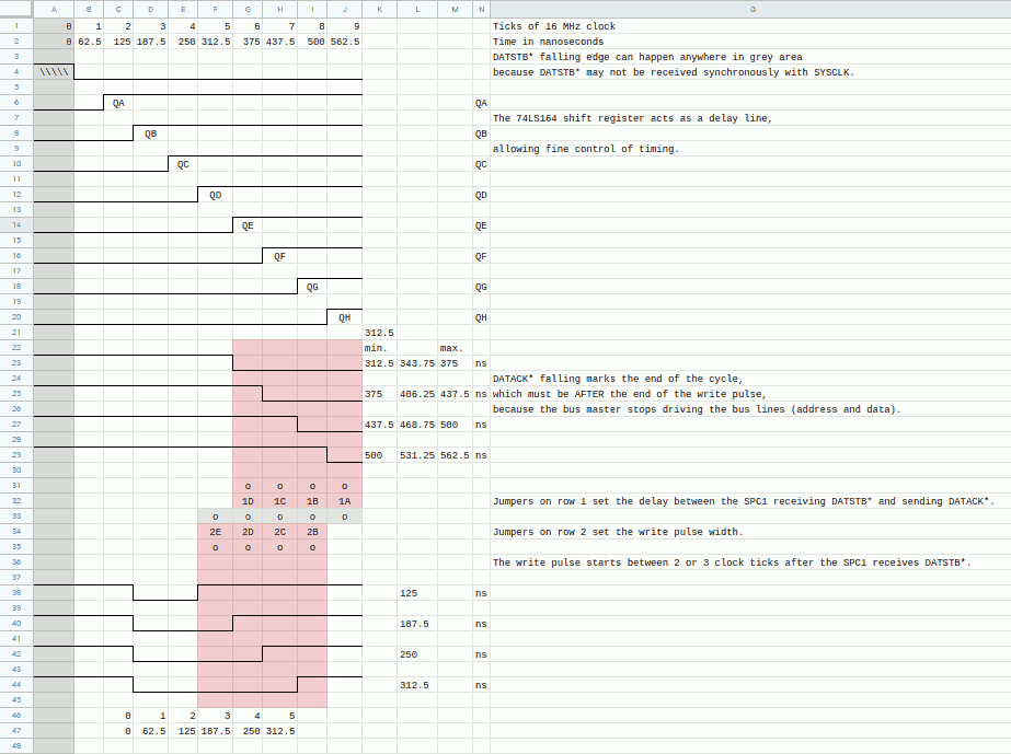
A shift register is a way to have well-controlled delays. The diagram below shows how a logic high ripples through a 74LS164 shift register (signals QA to QH) and produce the DATACK signal when desired.
As a bonus, they can be used to generate any timing pulse with a single AND gate and a NOT gate.
A common example is a write pulse that must start some time after the data is valid and end some time before the data goes invalid. The lower half of the diagram shows such signals. The short one is made by ANDing QB with NOT QD.
It is possible to create more complex signals with a little more logic. Such as signals that mimic those of a particular peripheral chip's processor family.
Discussions
Become a Hackaday.io Member
Create an account to leave a comment. Already have an account? Log In.