 jbb
jbbIn this entry we'll look at how to deploy MOSFETs in bridge circuits. (This is also applicable to IGBTs.)
Switch mode electronics are great - they are usually smaller and more efficient than similar linear circuits. However, there are some limitations that we must obey. This log is about how to drive a switch mode MOSFET driver stage.
While you're here, could someone please give me a comment about style? Am I writing too much or too little? Too formal?
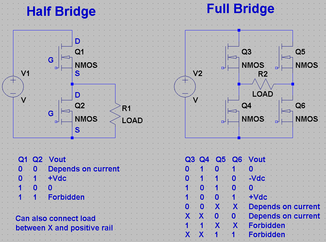
OK, now let's look at half and full bridge circuits. A half bridge has two switches (Q1 and Q2) and can produce two output voltages: 0 and Vdc. A full bridge has four switches (Q3 - Q6) and can produce three output voltages: -Vdc, 0 and + Vdc. There are some forbidden states which short-circuit the DC link and must be avoided. From a drive perspective, a full bridge is equivalent to two half bridges, so the rest of this article will look at half bridges exclusively.
So, how does a MOSFET work? There is quite a lot of information available online and in textbooks so I'm not going to do a big treatment. If we have a look at the MOSFET with our switchmode hat on, there are 4 distinct modes of operation (not 3 as many textbooks would have it).
It all depends on the gate-source voltage, Vgs, and the drain-source voltage, Vds, and something called the threshold voltage (Vth).
1) Off. This occurrs when the gate-source voltages is below the threshold voltage, i.e. Vgs < Vth
2) Linear mode. This occurrs when the MOSFET is partially turned on. In this mode, the MOSFET works like a current sink. Vgs >= Vth and Vds < (Vgs=Vth).
3) Saturation mode. This occurrs when the MOSFET is fully turned on, and the drain-source path behaves like a resistor - this is the Rds,on parameter that you will find on a power MOSFET datasheet. This also works in reverse - you can 'short circuit' the body diode (this is called syncronous rectification).
4) Diode mode. All MOSFETs have a built in body diode! When Vds is negative (and greater than one diode drop) the MOSEFT will conduct in diode mode. Vds < approx -0.6V.
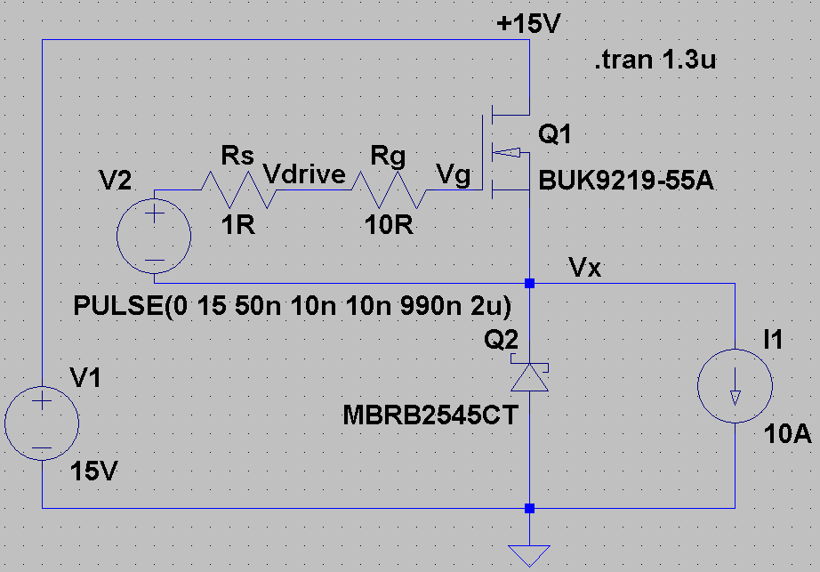
Now let's look at driving a MOSFET. I often use the circuit below to check switching waveforms. V1 is the main DC link (in a real circuit we'll need some capacitors!), V2 is the MOSFET gate driver (15V is a totally standard value, 'logic level' MOSFETs can be driven with 3.3V, 5V or 15V), and I1 is the load (equivalent to a nice big filter inductor, and very useful for evaluating performance in a simple, stable way). Initially, the MOSFET is off, and the diode is on. Vx is slightly lower (one diode drop) than ground.
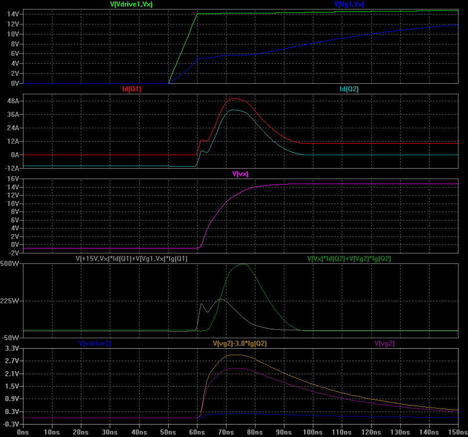
FYI: I picked the wrong MOSFET deliberately to give us some visible 'Miller plateaus.' You can do much better than this MOSFET.
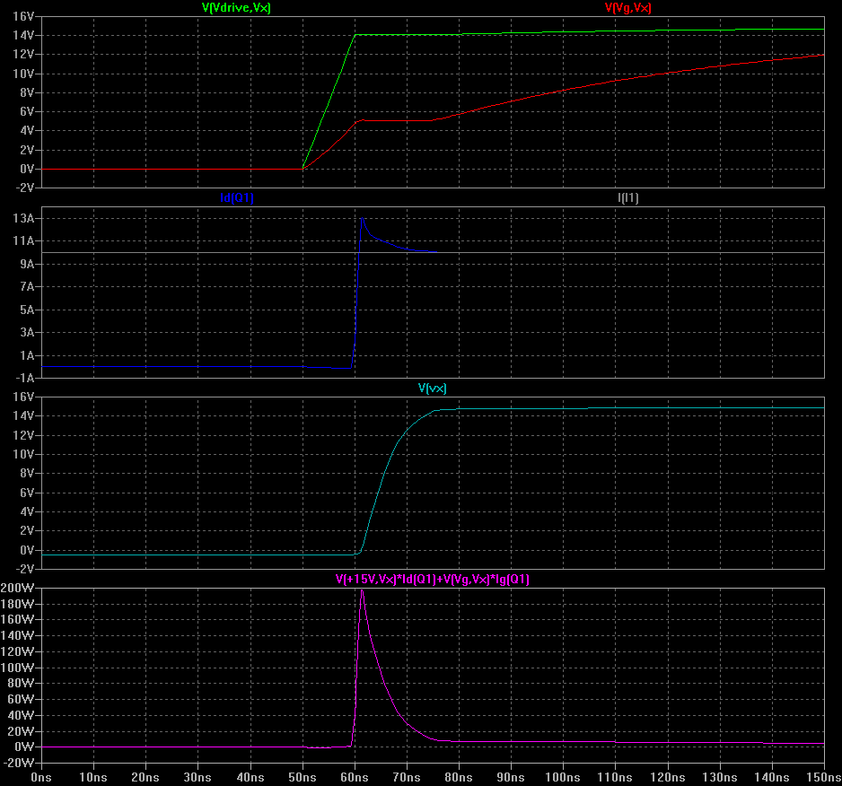
t0 - t1: (50 - 49 ns) When the driver switches on, the MOSFET Vgs climbs (note that there is internal capacitance). The time constant here is set by the internal MOSFET capacitance, the driver series resistance Rs (often in the 1R to 5R range) and the gate resistor Rg.
t1: (59ns) Vgs reaches Vth. Current begins to flow through the MOSFET drain pin.
t1 - t2: (59 - 61 ns) We are now in the linear mode. Current flow through the MOSFET rises. However, the switch node voltage Vx is not rising yet. Vgs continues to rise.
t3: (61 ns) Vgs is now high enough that the MOSFET can deliver the whole load current. Vds begins to fall / Vx begins to rise.
t3 - t4: (61 - 75 ns) Vds falls to zero / Vx rises to Vdc. During this time Vgs is basically flat. This is called the Miller Plateau, and is due to the Miller capacitance between the drain and gate. Current flows through this capacitance (in the 10s to 100s of pF range) in accordance with I = C * dv/dt and provides negative feedback. This is a very useful signal to look for when measuring prototypes.
t4: (75 ns) Vds falls to approximately zero: the MOSFET is turned on.
t4 - t5: (75 ns - 300 ns)Vgs rises a bit more, bringing the MOSFET on resistance down.
We see that quite a bit of power is dissipated in the MOSFET from t1 to t4. This is called the 'turn on loss,' and can be calculated by LTspice by Ctrl-clicking on the MOSFET power channel. Multiplying the turn on loss in Joules by the switching frequency in Hz (i.e. 1/s) gives the average switching loss in W - very useful. The MOSFET turn on loss is 1.1 uJ in this configuration, and the Miller plateau is approximately 14ns long, with an amplitude of 5V.
Wait a moment! The MOSFET current has an extra 3A high bump in it! (Around t = 61 ns) This is due to the reverse recovery and parasitic capacitance of the diode Q2 (Schottky, 45V / 25A). I used a Schottky to reduce the reverse recovery to zero, but it still has capacitance and dissipates about 0.1 uJ during the turn on process.
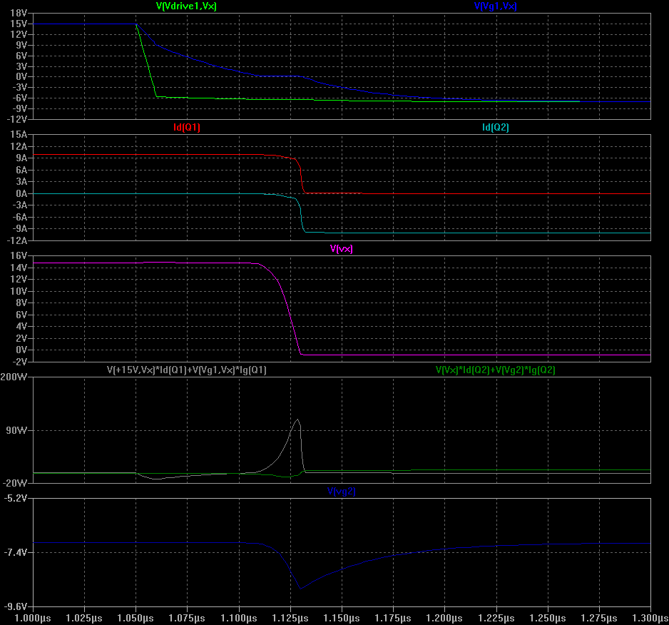
When the MOSFET switches off, the process happens in reverse (and yes, there are turn off losses). The Miller plateau is approximately 75ns long, and the turn-off loss is 4.5uJ - not so good as the turn on!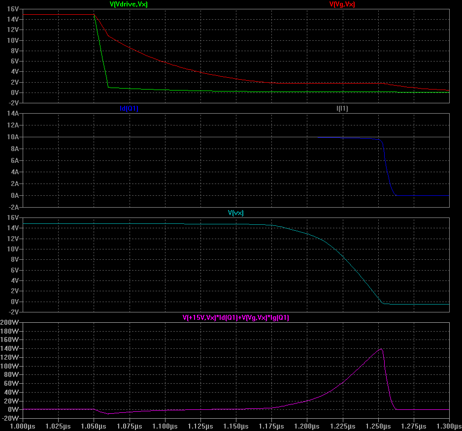 So the total on and off losses in Q1 are approximately 5.6 uJ. We can improve the situation, more on that later.
Summary: Q1 on+off = 5.6 uJ, Q2 rev. recov. = 0.1 uJ, grand total 5.7 uJ.
HALF BRIDGE GATE DRIVE
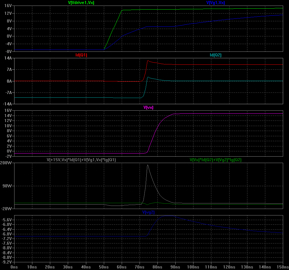
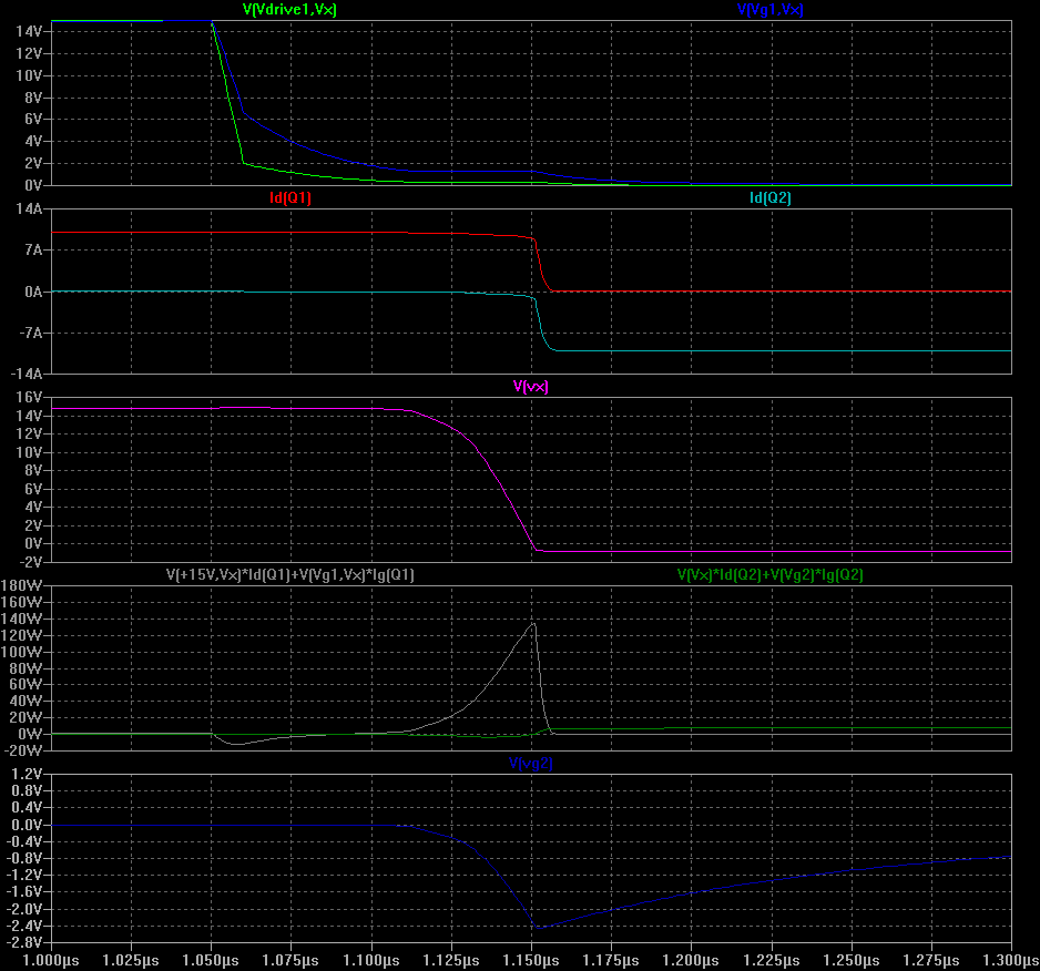
Now let's look at what happens with an actual half bridge configuration. Q2 is used as a diode here. 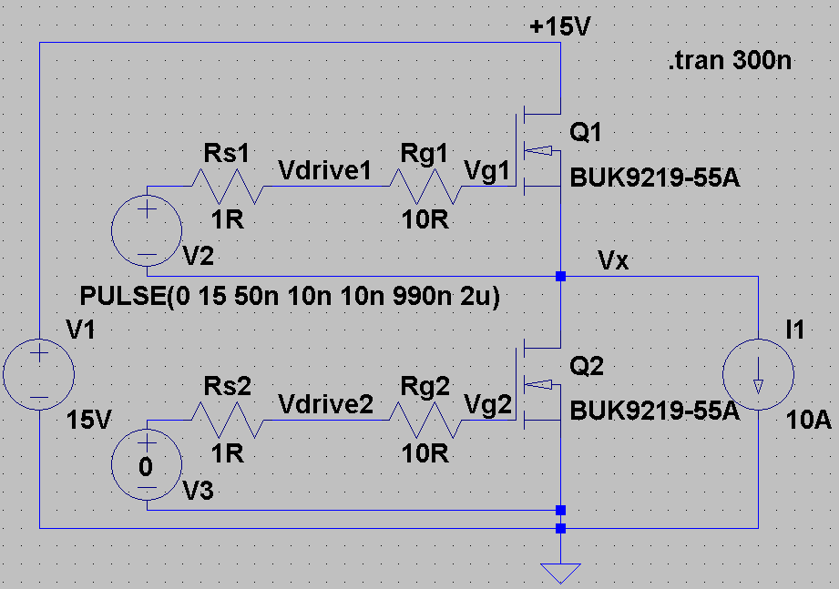
 Turn on of Q1: 3.5 uJ
'Reverse recovery' of Q2: 8.3uJ!!
The Miller plateau is 18ns, and the turn on losses are 3.5uJ in Q1. Why the increase? Because Q2 is misbehaving and has a big curent spike of about 40A (and associated losses thereof ). An essential thing to note is that Vg2 (bottom) does not stay at 0V but actually rises up to about 2V. This is due to coupling of the voltage change in Vx through the Miller capacitance (Cdg) of Q2, through Cdg * dVx / dt. This pushes some current through Q2's gate, and driver doesn't clamp it down hard enough. Q2 actually begins to conduct through the channel (that's where the 40A comes from); this is effectively short circuiting the supply via Q1 and Q2. This is called shoot-through and is very bad news: at best, it causes unneccessary losses. At worst, it
Additionally, these MOSFETs have some internal gate resistance (reading the Spice model, it's about 3 Ohms). If we add a little maths, ("V(vg) - 3.0*Ig(Q2)") we can get the 'effective' gave voltage... and see that it hits around 3.0V, which is definitely turning on Q2 at the worst possible time.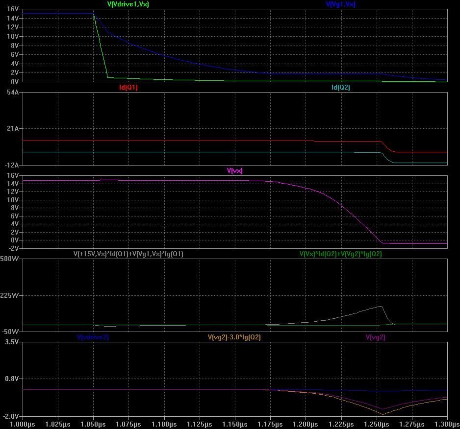
Turn off of Q1: 4.6uJ
Summary: Q1 on+off = 8.1 uJ, Q2 rev. recov. = 8.3 uJ, grand total 16.4 uJ.
During the turn-off of Q1, Q2 has no reverse recovery (there is such a thing as forward recovery, but it's usually negligible) and the switching loss is basically the same as with the Schottky.
NEGATIVE GATE DRIVE
We can use negative gate drive to try to fix Q2's bad behaviour. This involves using -7V/+15V for the gate drivers instead of 0V/+15V (see red circles in circuit diagram). It requires extra circuitry but is really effective. Almost all high power designs (especially those using IGBTs) will use this trick as it gives really good results. The turn-off losses improve too, because more current is available to suck charge out of Q1's gate during turn-off.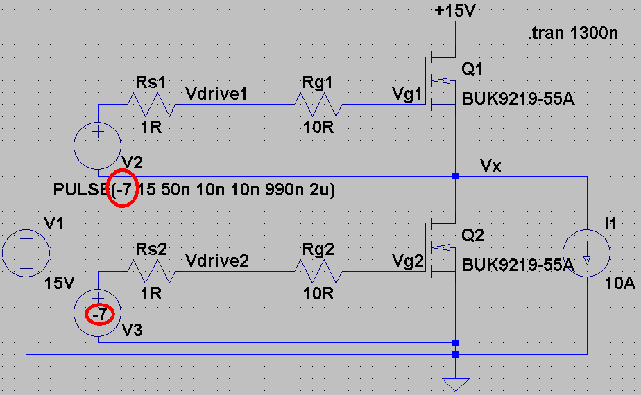
 Turn on of Q1: 1.2 uJ
Reverse recovery of Q2: 0.3 uJ
Turn off of Q2: 1.0 uJ
Summary: Q1 on+off = 2.2 uJ, Q2 rev. recov. = 0.3 uJ, grand total 2.5 uJ (way better than the previous half-bridge, and even better than the original MOSFET + Schottky).
MODIFIED GATE RESISTORS
A cheaper way to address the shoot through problem is to modify the gate resistors, as shown: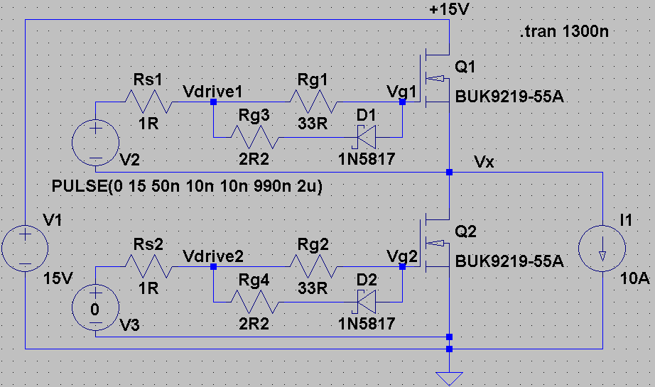
How did I select these values? Not so simply, sorry :-(. First, I decided that I would use a medium-large driver chip with a 2.5A 'sink' capability and about 1 Ohm of series resistance (you can find this info in MOSFET driver datasheets, I personally like the Si8233 range from Silabs, but they are a little pricey). Considering a +15V voltage swing out of the driver, with 1R in the driver chip and 3R in the MOSFET, I chose 2.2R for Rg3 and Rg4 to give approx 2.5A turn-off current (note that we really get 10R in parallel with 2.2R, i.e. 1.8R). Then I increased (running multiple simulations) Rg1 and Rg2 until the effective gate voltage (considering the 3R internal resistance!) was around 2.0V. Obviously, if you're doing this for a serious design you need to look in the datasheet at the minimum threshold voltage considering temperature - the threshold often drops with increasing temperature and you must consider that!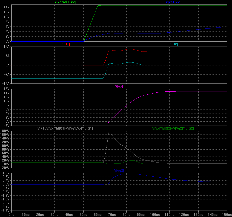 Turn on of Q1: 2.7 uJ
Reverse recovery of Q2: 0.4 uJ
 Turn off of Q2: 2.2 uJ
Summary: Q1 on+off = 4.7 uJ, Q2 rev. recov. = 0.4 uJ, grand total 5.1 uJ.
So, this trick is better than the initial circuit, but not so good as the negative gate drive version. It doesn't need a negative supply, though!
What else could we do to improve matters?
- Select a MOSFET with a higher threshold voltage. Many power MOSFETs have a threshold of around 5V which makes controlling shoot through easier.
- Select a driver chip with a 'Miller Clamp' built in, which is specifically designed to address this dV/dt induced turn on problem. Examples include the Avago ACPL-336.
Finally, if at all possible you should measure Vgs and Vds with a good scope (100MHz is marginal, 250MHz is better, and we use 1GHz ones at work) to make sure there's no funny business going on. Also make sure your probe is up to the job, properly connected and properly compensated (I'll try to find a link to a good article for this). If you've really got to be sure, measure Id as well - but you'll need a good current probe. Keep your layout really tight - any inductance in these circuits will lead to additional losses, possible device failure and electromagnetic interference.
At low voltages, MOSFET body diodes are OK in terms of reverse recovery. If you are moving up to higher voltages (say 380V DC), you must be _very_ careful about the reverse recover behaviour of MOSFETs and diodes. A standard MOSFET half-bridge at these voltages can literally explode if you haven't got the gate drive right. Sometimes you find that the turn-on resistors need to be so large (to control reverse recovery) that the switching losses are unacceptable. In this case there are a few things you can try:
1) switch to the CoolMOS CFD types, which have better than average body diodes
2) switch to IGBTs. These devices don't have a body diode (but CANNOT be operated with reverse voltages, sorry) are usually co-packaged with a separate diode chip (usually much better than a MOSFET body diode)
3) modify your topology so that you don't need half-bridges
4) mix MOSFETs and IGBTs (for experts, can be very effective, seen in several high-efficiency solar inverters)
5) use a soft-switching topology that avoids reverse recovery events.
Discussions
Become a Hackaday.io Member
Create an account to leave a comment. Already have an account? Log In.