Richard Coleman
Notes
This is a work in progress. Nothing here is final, and things can (and will) change radically before R1 is complete.
This project is public domain, in hardware and software / firmware. Design files are available from the sidebar on the project's homepage. These are updated as and when they are saved — as soon as I save an edit, it is available.
Ranges
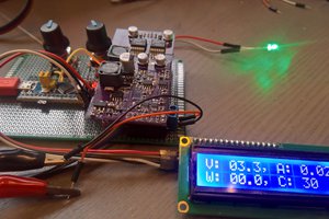
Ranges start from 0 volts / amps / ohms / watts; offset is calibrated out at the load's startup.
| Range | Resolution | Limit | Max offset | Accuracy | Note |
| Current | 1mA | 20A | 1mA | TBD | Hardware controlled |
| Voltage | 10mV | 100V | 10mV | ±0.1% ± 0.1% FS | Hardware controlled |
| Power | 10mW | 300W | 10mW | TBD | Software controlled. Measures current, then sets voltage according to V=P/I. |
| Resistance | 100mΩ | 1000Ω | 100mΩ | TBD | Software controlled. Measures current, then sets voltage according to V=IR |
Accuracy figures most ranges are not yet available, but are likely to be slightly lower (i.e., poorer) than those of the voltage range. They will depend upon the specific current shunt used, among other things.
Components
| Microcontroller | Psoc 4200 (4$ prototyping kit) — ARM Cortec M0+ |
| Analog multiplexer | Psoc 4200 (4$ prototyping kit) — ARM Cortec M0+ |
| ADC | ADC16S626 |
| DAC | DAC7562/3 (12 bits, DAC7562 preferred) |
| P-channel power MOSFETs | IXTH75N10L2 |
| Voltage reference | REF5040 (0.05%, 3ppm/C drift, 8.8uV RMS noise) |
| Op-amps | OPA4188 (6-25uV offset, extremely low drift) |
Design
Tools
The load is being designed in KiCad, an open-source EDA package. It is designed on bleeding-edge builds as the latest stable builds are several years old. The latest design files can be found on the sidebar of the project's homepage.
P-channel power MOSFETs
Traditional MOSFETs are not rated for DC (continuous) use, so their Safe Operating Area (SOA) is limited for any period longer than 100ms. This means they will not cope with dissipating high levels of power (such as those generated by a load) continuously. To get around this problem, this design uses IXYS Linear L2 MOSFETs which are specifically designed for continuous DC use, allowing it to reach 300W power dissipation with only two MOSFETs.
DAC
The DAC's LSB (least significant bit) is dithered to provide 3 extra bits of resolution.
For those who aren't aware, this means that the LSB functions as a PWM: the percentage of time that it's on per second corresponds to the output. The DAC's output has to be fed through a low-pass filter.
Dithering makes the DAC practically equivalent to a 15-bit DAC, but with a reduced sample rate of 12.5 kSps max (reduction in sample rate is 2^n where n is the number of extra bits). Since the fastest that the DAC needs to sample is 1kHz, the dithering has plenty of time to take place.
Dithering also allows for software offset nulling by allowing much smaller increments in the output.
Voltage reference
The load needs a 3.2768V reference since it is running at a 15-bit resolution. This allows the DAC to output from 0V (+ offset) to 3.2768V in steps of 100uV. The DAC7563 has a decent internal voltage reference, but it is fixed at 2.5V. Because of this, the load uses a REF5040. This provides better accuracy and drift, and since it is 4.096V only a voltage divider (ratio 1:4) is required to drop it to 3.2768V.
ADC
The PSoC's internal ADC is excellent, but it's 12-bit. Unlike with the DAC, oversampling would probably not be accurate enough, so instead an external ADC is used.
Current sensing
High-accuracy high-power low-tempco shunts are expensive, so instead two very low value (10 mOhm) shunts are used with super-low offset op-amps to provide a current sense channel for each power MOSFET.
Voltage sensing
The input voltage is fed through a voltage divider with a ratio of 100:1, i.e., 100V in means 1V out. This then goes through some protection, and to the ADC. The ADC measures up to 3.2768V, so taking into account the voltage divider, it measures in 10mV increments.
Offset
The DAC has an inherent offset of a few millivolts. Fortunately, this can be removed by using one of the DAC's outputs as a nulling output. The nulling output is subtracted from...
Read more »
 Radu Motisan