 Tim Vaughan
-
1Step 1
Setting up the hardware
There are a few things to know about the LC STUDIO module:
- The two rows of header pins on the board are exactly the same. Each column contains a pair of pins connected to one another. This means that the board is breadboard compatible. The only tricky thing there is that the pin descriptions are silk-screened onto the front of the board, which is not visible when the board is plugged into a breadboard.
- The board supplies SD cards with 3.3v via a LM1117 linear regulator. Both of the pins labelled 3.3v and 5.5v are connected to the input pin of this regulator, so you can feed the supply voltage to either of them.
- The board does not do any level shifting on the SPI pins, so you need to supply 3.3v there. (This is very annoying, but I can't really complain given how inexpensive these boards are.)
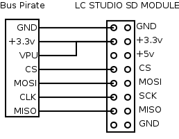
With these things in mind, we can (using a breadboard) connect the Bus Pirate to the module in the following way:
![]()
Note that we're using the 3.3v supply to power the module, and we're also connecting this to the Vpu pin on the BP. We do this because we're going to use the open drain form of the BP's SPI mode.
In addition, I've connected inputs 0 through 3 of my Logic Pirate to MISO, CLK, MOSI and CS. This will give me a nice low-level view of what's going on.
Once that's all in place, we finally insert our SDHC card into the module's socket. -
2Step 2
Initializing the Bus Pirate
With BP hardware version 3.b and firmware version 6.1, the default SPI mode parameters are all that's required to speak with the SD card. Following a BP reset or power up, the following is sufficient to set up the BP:
HiZ>m
1. HiZ
2. 1-WIRE
3. UART
4. I2C
5. SPI
6. 2WIRE
7. 3WIRE
8. LCD
x. exit(without change)

(1)>5
Set speed:
 1. 30KHz
 2. 125KHz
 3. 250KHz
 4. 1MHz

(1)>
Clock polarity:
 1. Idle low *default
 2. Idle high

(1)>
Output clock edge:
 1. Idle to active
 2. Active to idle *default

(2)>
Input sample phase:
 1. Middle *default
 2. End

(1)>
CS:
 1. CS
 2. /CS *default

(2)>
Select output type:
 1. Open drain (H=Hi-Z, L=GND)
 2. Normal (H=3.3V, L=GND)

(1)>
Ready
SPI>
Note that I've just hit Enter all prompts save the first.
Now we turn on the on-board BP power supplies and activate the pull-up resistors:
SPI>W
POWER SUPPLIES ON
SPI>P
Pull-up resistors ON
SPI>
We're now ready to start talking SPI to the SD card. -
3Step 3
Putting the card in SPI mode
SD cards are conversant in two different protocols: a native high-speed protocol and a low-speed SPI protocol. The SPI protocol is supported to make it easy for microcontrollers to store and retrieve data from the cards. However, once powered up the cards default to the higher speed protocol. We therefore have to explicitly tell the card that we wish to speak SPI.
The procedure for doing this is quite straight forward, although there are a number of steps. It is described in full in the Physical Layer Simplified Specification. One of the main reasons for writing this mini-guide is to record the initialization steps I finally used.
Firstly, some background. Each SD card command has an index running from 0 through 63. Each command is issued by sending 6 bytes via SPI to the card, with the CS line held LOW. The first of these is 0x40 ORed with the command index. The next four are arguments to the command or zero if no argument is required. The last byte is a CRC value computed from the 5 command bytes. (The algorithm for computing this value is described in the spec, but it is not straightforward to compute by hand. A tiny C++ program for computing these values can be found at https://github.com/hazelnusse/crc7.)
The first command we issue is CMD0, which resets the SD card:
SPI>] r:8 [ 0x40 0 0 0 0 0x95 r:8 ]
/CS DISABLED
READ: 0xFF 0xFF 0xFF 0xFF 0xFF 0xFF 0xFF 0xFF
/CS ENABLED
WRITE: 0x40
WRITE: 0x00
WRITE: 0x00
WRITE: 0x00
WRITE: 0x00
WRITE: 0x95
READ: 0xFF 0x01 0xFF 0xFF 0xFF 0xFF 0xFF 0xFF
/CS DISABLED
SPI>
The "] r:8" at the beginning gives the card some clock cycles to finish doing anything it may have been doing before we issue the command. "[" causes the CS line to be brought low, after which we send the 6 command bytes (the 6th 0x95 being the CRC value for the command). We then read in 8 bytes before sending the CS line high again.The second byte read is the command response. The format for this response (an "R1" response) is described in the spec. The value 0x01 means that the reset command succeeded and the card is in the IDLE state.
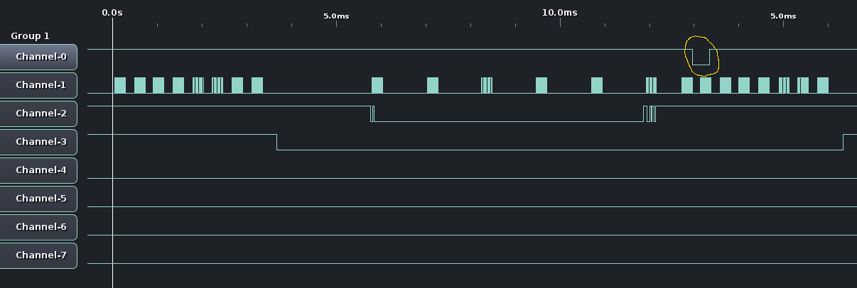
Getting this far is actually a minor victory in itself, as it means that we've successfully used the LC STUDIO module to connect to the card. Using the Logic Pirate to look at the above exchange, we see the following:
![]() Channel 0 is MISO, channel 1 is the clock, 2 is MOSI and 3 is CS. The trace circled in yellow is the SD card responding to our reset command. (It's ALIVE!)
Channel 0 is MISO, channel 1 is the clock, 2 is MOSI and 3 is CS. The trace circled in yellow is the SD card responding to our reset command. (It's ALIVE!)The second command we send is CMD8. This is required for newer SD cards and lets us inform the card of the voltage we are operating at, giving the card a chance to tell us whether this is ok. We pass an argument of 0x00 0x00 0x01 0xAA. The 0x01 specifies a desired operating voltage range of 2.7v to 3.6v. The 0xAA is a "check pattern" that will be echoed back by the card on success. The following shows how this command is sent using the BP:
SPI>[ 0x48 0 0 0x01 0xaa 0x87 r:8 ]
/CS DISABLED
READ: 0xFF 0xFF 0xFF 0xFF 0xFF 0xFF 0xFF 0xFF
/CS ENABLED
WRITE: 0x48
WRITE: 0x00
WRITE: 0x00
WRITE: 0x01
WRITE: 0xAA
WRITE: 0x87
READ: 0xFF 0x01 0x00 0x00 0x01 0xAA 0xFF 0xFF
/CS DISABLED
SPI>
The response format is "R7" which includes an "R1" as its first byte: hence the first "0x01" in the response. Following a few zeros, we see another 0x01 indicating that the voltage range is accepted, as well as the check pattern 0xAA echoed back, indicating success.The next command we send is CMD59 to turn off the CRC checking. This makes issuing subsequent commands much easier, as we no longer have to compute these values. The CRC for CMD59 however must still be correct:
] r:8 [ 0x7b 0 0 0 0 0x91 r:8 ]
/CS DISABLED
READ: 0xFF 0xFF 0xFF 0xFF 0xFF 0xFF 0xFF 0xFF
/CS ENABLED
WRITE: 0x7B
WRITE: 0x00
WRITE: 0x00
WRITE: 0x00
WRITE: 0x00
WRITE: 0x91
READ: 0xFF 0x01 0xFF 0xFF 0xFF 0xFF 0xFF 0xFF
/CS DISABLED
SPI>
Again we see an R1 response indicating that the card remains in the idle state.Next is CMD58 which is used to check the contents of the OCR (operating conditions register):SPI>] r:8 [ 0x7a 0 0 0 0 0 r:8 ] /CS DISABLED READ: 0xFF 0xFF 0xFF 0xFF 0xFF 0xFF 0xFF 0xFF /CS ENABLED WRITE: 0x7A WRITE: 0x00 WRITE: 0x00 WRITE: 0x00 WRITE: 0x00 WRITE: 0x00 READ: 0xFF 0x01 0x00 0xFF 0x80 0x00 0xFF 0xFF /CS DISABLED SPI>I don't actually know if this is required for initialization, but it's in the spec. You could try leaving it out.Lastly, we need to issue the application-specific command ACMD41. Application-specific commands are issued by first issuing CMD55 followed by a command with index 41 (it would be CMD41 if not for the CMD55 prefix). The 30th bit in the ACMD41 argument is used to specify whether the host (that's us!) supports high-capacity cards. We need to set this bit, otherwise the command will return an error as this is an SDHC card. The command is issued as follows:
SPI>] r:8 [ 0x77 0 0 0 0 0 r:8 ]
/CS DISABLED
READ: 0xFF 0xFF 0xFF 0xFF 0xFF 0xFF 0xFF 0xFF
/CS ENABLED
WRITE: 0x77
WRITE: 0x00
WRITE: 0x00
WRITE: 0x00
WRITE: 0x00
WRITE: 0x00
READ: 0xFF 0x01 0xFF 0xFF 0xFF 0xFF 0xFF 0xFF
/CS DISABLED
SPI>] r:8 [ 0x69 0x40 0 0 0 0 r:8 ]
/CS DISABLED
READ: 0xFF 0xFF 0xFF 0xFF 0xFF 0xFF 0xFF 0xFF
/CS ENABLED
WRITE: 0x69
WRITE: 0x40
WRITE: 0x00
WRITE: 0x00
WRITE: 0x00
WRITE: 0x00
READ: 0xFF 0x01 0xFF 0xFF 0xFF 0xFF 0xFF 0xFF
/CS DISABLED
SPI>
Note that the R1 response of ACMD41 is still 0x01, indicating a card in the idle state. This response indicates that the card is still initializing. We repeat ACMD41 until we see a response of 0x00:SPI>] r:8 [ 0x77 0 0 0 0 0 r:8 ] r:8 [ 0x69 0 0 0 0 0 r:8 ] /CS DISABLED READ: 0xFF 0xFF 0xFF 0xFF 0xFF 0xFF 0xFF 0xFF /CS ENABLED WRITE: 0x77 WRITE: 0x00 WRITE: 0x00 WRITE: 0x00 WRITE: 0x00 WRITE: 0x00 READ: 0xFF 0x01 0xFF 0xFF 0xFF 0xFF 0xFF 0xFF /CS DISABLED READ: 0xFF 0xFF 0xFF 0xFF 0xFF 0xFF 0xFF 0xFF /CS ENABLED WRITE: 0x69 WRITE: 0x00 WRITE: 0x00 WRITE: 0x00 WRITE: 0x00 WRITE: 0x00 READ: 0xFF 0x00 0xFF 0xFF 0xFF 0xFF 0xFF 0xFF /CS DISABLED SPI>Got it in one! Note that we don't have to worry about the argument to subsequent ACMD41s - only the first one matters. (This cuts both ways - if you stuff up the argument on the first call to ACMD41 you'll need to start over.)We now have an SD card successfully initialized in SPI mode.
-
4Step 4
Reading from the SDHC card
To demonstrate that we can successfully read from the card, we use the read single block command CMD17.
SPI>] r:8 [ 0x51 0 0 0 0 0 r:550 ]
/CS DISABLED
READ: 0xFF 0xFF 0xFF 0xFF 0xFF 0xFF 0xFF 0xFF
/CS ENABLED
WRITE: 0x51
WRITE: 0x00
WRITE: 0x00
WRITE: 0x00
WRITE: 0x00
WRITE: 0x00
READ: 0xFF 0xFF 0x00 0xFF 0xFF 0xFF 0xFF 0xFF 0xFF 0xFF 0xFF 0xFF 0xFF 0xFF 0xFF 0xFF 0xFF 0xFE 0xFA 0xB8 0x00 0x10 0x8E 0xD0 0xBC 0x00 0xB0 0xB8 0x00 0x00 0x8E 0xD8 0x8E 0xC0 0xFB 0xBE 0x00 0x7C 0xBF 0x00 0x06 0xB9 0x00 0x02 0xF3 0xA4 0xEA 0x21 0x06 0x00 0x00 0xBE 0xBE 0x07 0x38 0x04 0x75 0x0B 0x83 0xC6 0x10 0x81 0xFE 0xFE 0x07 0x75 0xF3 0xEB 0x16 0xB4 0x02 0xB0 0x01 0xBB 0x00 0x7C 0xB2 0x80 0x8A 0x74 0x01 0x8B 0x4C 0x02 0xCD 0x13 0xEA 0x00 0x7C 0x00 0x00 0xEB 0xFE 0x00 0x00 0x00 0x00 0x00 0x00 0x00 0x00 0x00 0x00 0x00 0x00 0x00 0x00 0x00 0x00 0x00 0x00 0x00 0x00 0x00 0x00 0x00 0x00 0x00 0x00 0x00 0x00 0x00 0x00 0x00 0x00 0x00 0x00 0x00 0x00 0x00 0x00 0x00 0x00 0x00 0x00 0x00 0x00 0x00 0x00 0x00 0x00 0x00 0x00 0x00 0x00 0x00 0x00 0x00 0x00 0x00 0x00 0x00 0x00 0x00 0x00 0x00 0x00 0x00 0x00 0x00 0x00 0x00 0x00 0x00 0x00 0x00 0x00 0x00 0x00 0x00 0x00 0x00 0x00 0x00 0x00 0x00 0x00 0x00 0x00 0x00 0x00 0x00 0x00 0x00 0x00 0x00 0x00 0x00 0x00 0x00 0x00 0x00 0x00 0x00 0x00 0x00 0x00 0x00 0x00 0x00 0x00 0x00 0x00 0x00 0x00 0x00 0x00 0x00 0x00 0x00 0x00 0x00 0x00 0x00 0x00 0x00 0x00 0x00 0x00 0x00 0x00 0x00 0x00 0x00 0x00 0x00 0x00 0x00 0x00 0x00 0x00 0x00 0x00 0x00 0x00 0x00 0x00 0x00 0x00 0x00 0x00 0x00 0x00 0x00 0x00 0x00 0x00 0x00 0x00 0x00 0x00 0x00 0x00 0x00 0x00 0x00 0x00 0x00 0x00 0x00 0x00 0x00 0x00 0x00 0x00 0x00 0x00 0x00 0x00 0x00 0x00 0x00 0x00 0x00 0x00 0x00 0x00 0x00 0x00 0x00 0x00 0x00 0x00 0x00 0x00 0x00 0x00 0x00 0x00 0x00 0x00 0x00 0x00 0x00 0x00 0x00 0x00 0x00 0x00 0x00 0x00 0x00 0x00 0x00 0x00 0x00 0x00 0x00 0x00 0x00 0x00 0x00 0x00 0x00 0x00 0x00 0x00 0x00 0x00 0x00 0x00 0x00 0x00 0x00 0x00 0x00 0x00 0x00 0x00 0x00 0x00 0x00 0x00 0x00 0x00 0x00 0x00 0x00 0x00 0x00 0x00 0x00 0x00 0x00 0x00 0x00 0x00 0x00 0x00 0x00 0x00 0x00 0x00 0x00 0x00 0x00 0x00 0x00 0x00 0x00 0x00 0x00 0x00 0x00 0x00 0x00 0x00 0x00 0x00 0x00 0x00 0x00 0x00 0x00 0x00 0x00 0x00 0x00 0x00 0x00 0x00 0x00 0x00 0x00 0x00 0x00 0x00 0x00 0x00 0x00 0x00 0x00 0x00 0x00 0x00 0x00 0x00 0x00 0x00 0x00 0x00 0x00 0x00 0x00 0x00 0x00 0x00 0x00 0x00 0x00 0x00 0x00 0x00 0x00 0x00 0x00 0x00 0x00 0x00 0x00 0x00 0x00 0x00 0x00 0x00 0x00 0x00 0x00 0x00 0x00 0x00 0x00 0x00 0x00 0x00 0x00 0x00 0x00 0x00 0x00 0x00 0x00 0x00 0x00 0x00 0x00 0x00 0x00 0x00 0x00 0x00 0x00 0x00 0x00 0x00 0x00 0x00 0x00 0x71 0x34 0x0A 0x00 0x00 0x00 0x00 0x01 0x01 0x00 0x83 0xFE 0xFF 0xC5 0x3F 0x00 0x00 0x00 0x07 0xCC 0xEC 0x00 0x00 0x00 0x00 0x00 0x00 0x00 0x00 0x00 0x00 0x00 0x00 0x00 0x00 0x00 0x00 0x00 0x00 0x00 0x00 0x00 0x00 0x00 0x00 0x00 0x00 0x00 0x00 0x00 0x00 0x00 0x00 0x00 0x00 0x00 0x00 0x00 0x00 0x00 0x00 0x00 0x00 0x00 0x00 0x00 0x00 0x00 0x00 0x00 0x55 0xAA 0xA4 0x3D 0xFF 0xFF 0xFF 0xFF 0xFF 0xFF 0xFF 0xFF 0xFF 0xFF 0xFF 0xFF 0xFF 0xFF 0xFF 0xFF 0xFF 0xFF
/CS DISABLED
SPI>
The card responds with a successful R1, followed by the first 512 byte block of the card. The start of the block is marked by the first 0xFE, and the block ends with a checksum of the retrieved data.Success!
Read from SDHC card using Bus Pirate
Details of how I succeeded in reading from an SDHC card using the BP and an LC STUDIO module/breakout.
 Channel 0 is MISO, channel 1 is the clock, 2 is MOSI and 3 is CS. The trace circled in yellow is the SD card responding to our reset command. (It's ALIVE!)
Discussions
Become a Hackaday.io Member
Create an account to leave a comment. Already have an account? Log In.