 Dave
DaveArtemis!
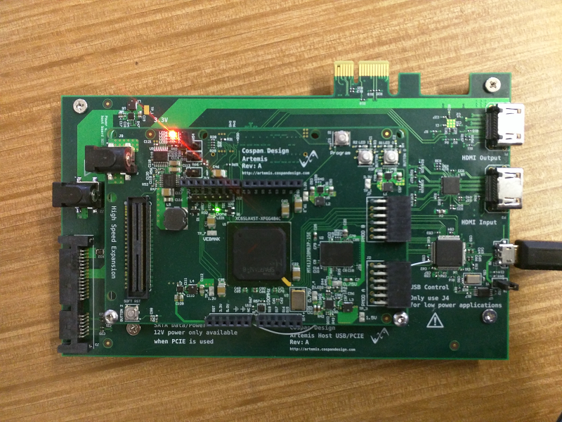
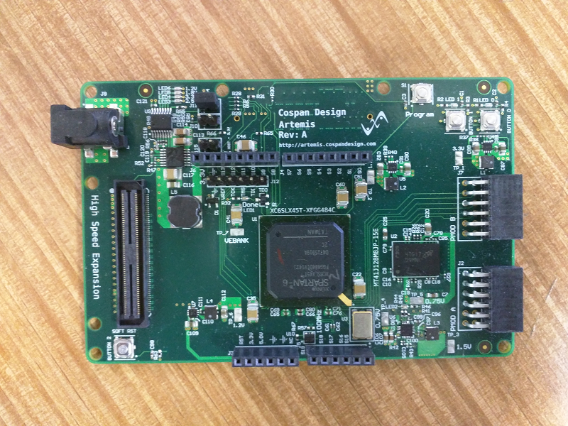 Artemis attached to the USB 2.0 and PCI Express Board
FAB to Assembly
Artemis came from fab about two months ago. I had hoped I could assemble the entire board myself in order to save some money. The FPGA and DDR3 came pre-balled with ROHS (lead free) solder so I didn't need to put down any solder paste. So I put the FPGA and memory chip on the board and ran it through the reflow oven. It looked like it worked until I bumped the board and both chips fell off.
After a couple more attempts I asked my friend at MIT Media Lab to let me use the BGA rework station. We spent half a day there putting on FPGAs and memory chip. It looked like it worked so I went to ahead assembling the rest of the board. It was about 1 AM and I was nearly finished when I looked down at the board and noticed the DDR3 had slid sideways... the DDR3 didn't stick then either. I tentatively tested the FPGA and it was only attached by a couple of balls... GRRR!
I decided to bite the bullet and spend about $1,000 to get the boards assembled.
Smoke to Nysa
Finally it was time for the smoke test. Success! Artemis held onto it's smoke. All regulators were outputting the correct voltages. I moved on to testing the FPGA. I created a simple LED blink app to test out the FPGA, LEDs, buttons and 100MHz oscillator. Success! I attached the new host interface board and after about a week of modifying a controller I used to interface with Dionysus I was able to download my first Nysa image. It was about that time I realized that I made a mistake in the design of Artemis... NO RESET BUTTON! ARGGH! I had to add an external wire but the correct solution is to add a open drain reset signal will pull the pre-existing reset pin on the Artemis base low from the host computer. This is useful so that I don't have to physically reset the board all the time.
DDR3
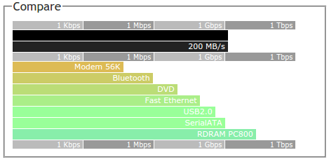
Dionysus, the small board I used to test out Nysa, had a 16-bit 100MHz SDRAM chip as the memory source. To get an idea of what is possible with SDRAM I generated the following comparison charge using this great website: Forret Tools
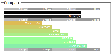
The DDR3 is obviously faster, it has an 8-bit interface at a double data rate running at 300MHz, so it equates to 1 byte @ 600MHz or this new comparison:
I used the built in DDR3 memory core generator from Xilinx Coregen to create and interface with the memory, then wrote a wishbone wrapper around it and after about a week I verified that I could write to all 128MB and read it back correctly!
I did run into an issue that I wanted to mention. Xilnx Coregen generates Verilog source code that I am not legally allowed to distribute so I figured out a way to generate a NGC file that users can instantiate. Its the equivalent of distributing a binary version of a library.
What next
I realized that in order to take advantage of the DDR3 I needed to design a DMA controller that could pull data from something like a camera put it into DDR3 memory temporarily and then store it into the SATA hard drives or output it to HDMI. It has turned out to be a complicated core. Once this is finished I am planning to design a stereo CSI camera board to test it out.
Discussions
Become a Hackaday.io Member
Create an account to leave a comment. Already have an account? Log In.