0%
0%
using_8085_processor_for_something
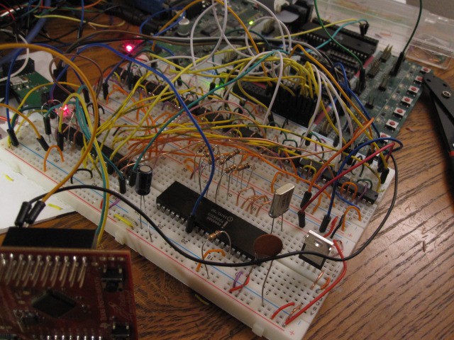
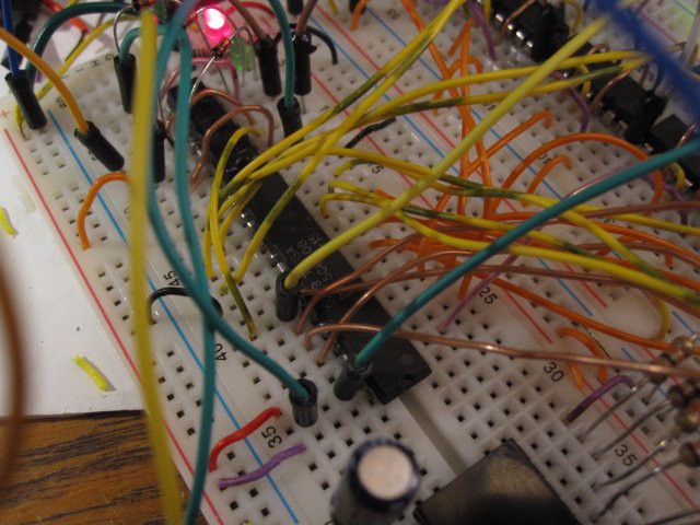
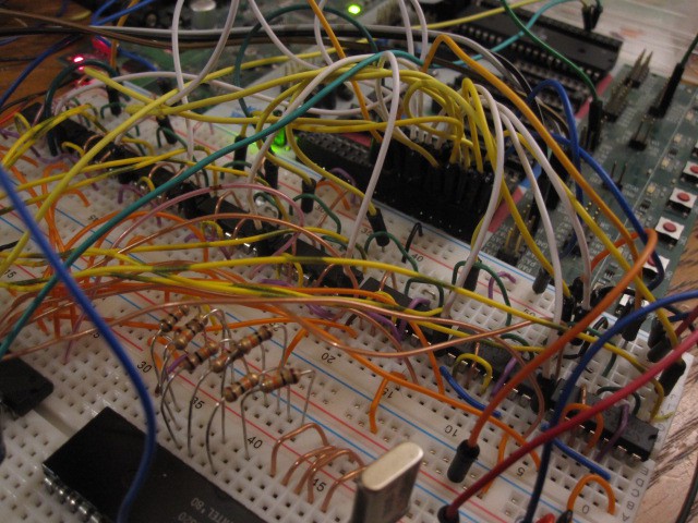
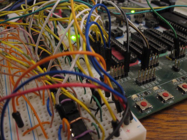
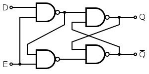
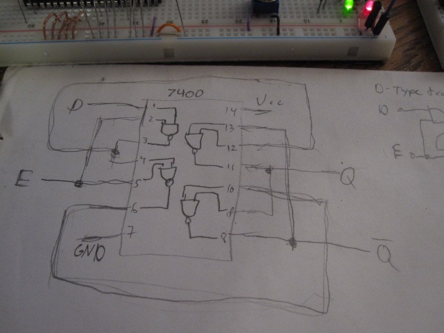
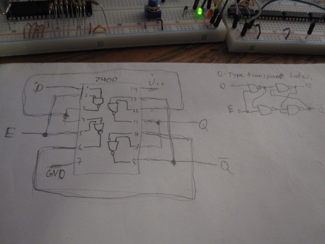
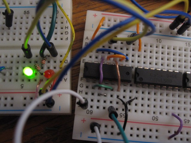
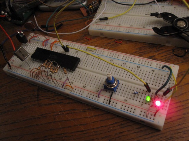
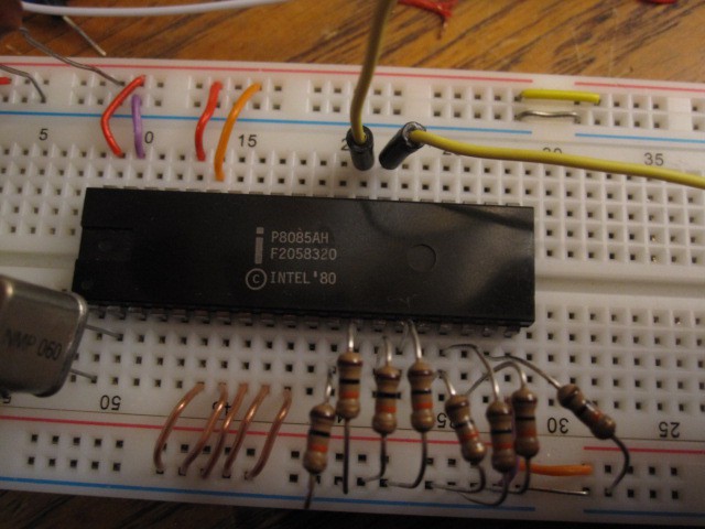
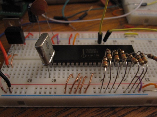
Project to try to figure out and do something with an Intel P8085 processor that I salvaged. Building a minimal 8-bit computer.
 Ethan Durrant
Become a Hackaday.io member
Already have an account? Log in.
Just one more thing
To make the experience fit your profile, pick a username and tell us what interests you.
Pick an awesome username
hackaday.io/
Your profile's URL: hackaday.io/username. Max 25 alphanumeric characters.
Pick a few interests
Projects that share your interests
People that share your interests
 Michael Möller
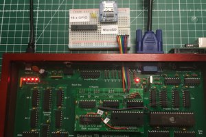
 Marcel van Kervinck
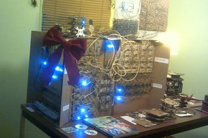
 Dr. Cockroach
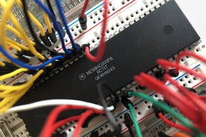
 Roman Romanchuk