Close
0%
0%

Arduino-Compatible FPGA Shield

Spartan 6 FPGA Shield includes SPI Configuration Flash, Breakout Headers, SRAM, programmable from Arduino or SPI Programmer

Similar projects worth following

Motivated by an interest in teaching folks how to use FPGAs and espouse the virtues of FPGA-coolness (& like many, frustrated a bit by a number of limitations of the Arduino incl. IO, peripherals, etc) I’ve endeavored to create the first (that I know of) FPGA-based Arduino shield.


This board - which I'm documenting here as I go along - includes heaps of additional IO, memory resources, etc. and is SPI programmable via SPI flash (including programming from the Arduino Due)...And is just an all-round cool way to introduce programmable device technology (beyond simple logic) to the uninitiated.

Likewise, it will have more than enough grunt for the old-pro to hack together some totally awesome, totally re-configurable systems.  

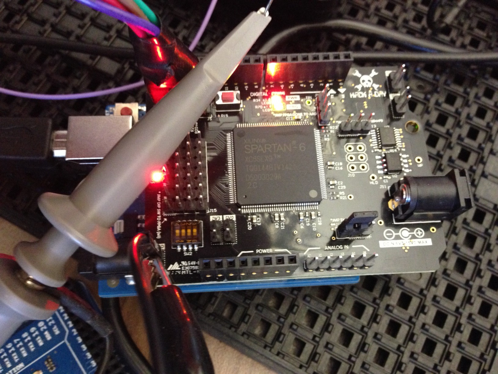
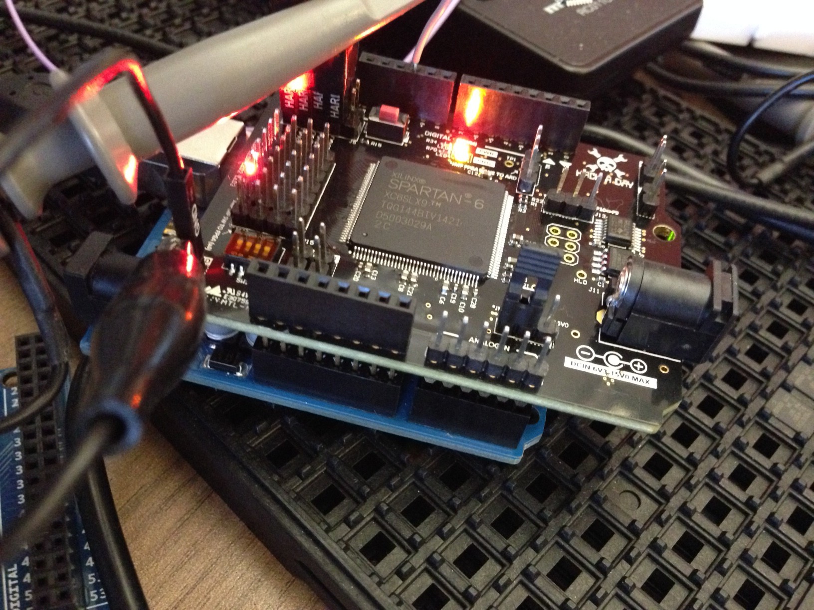
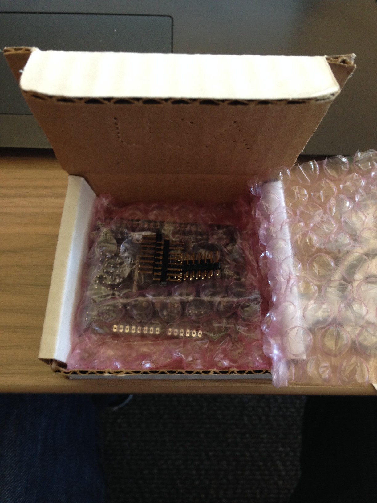
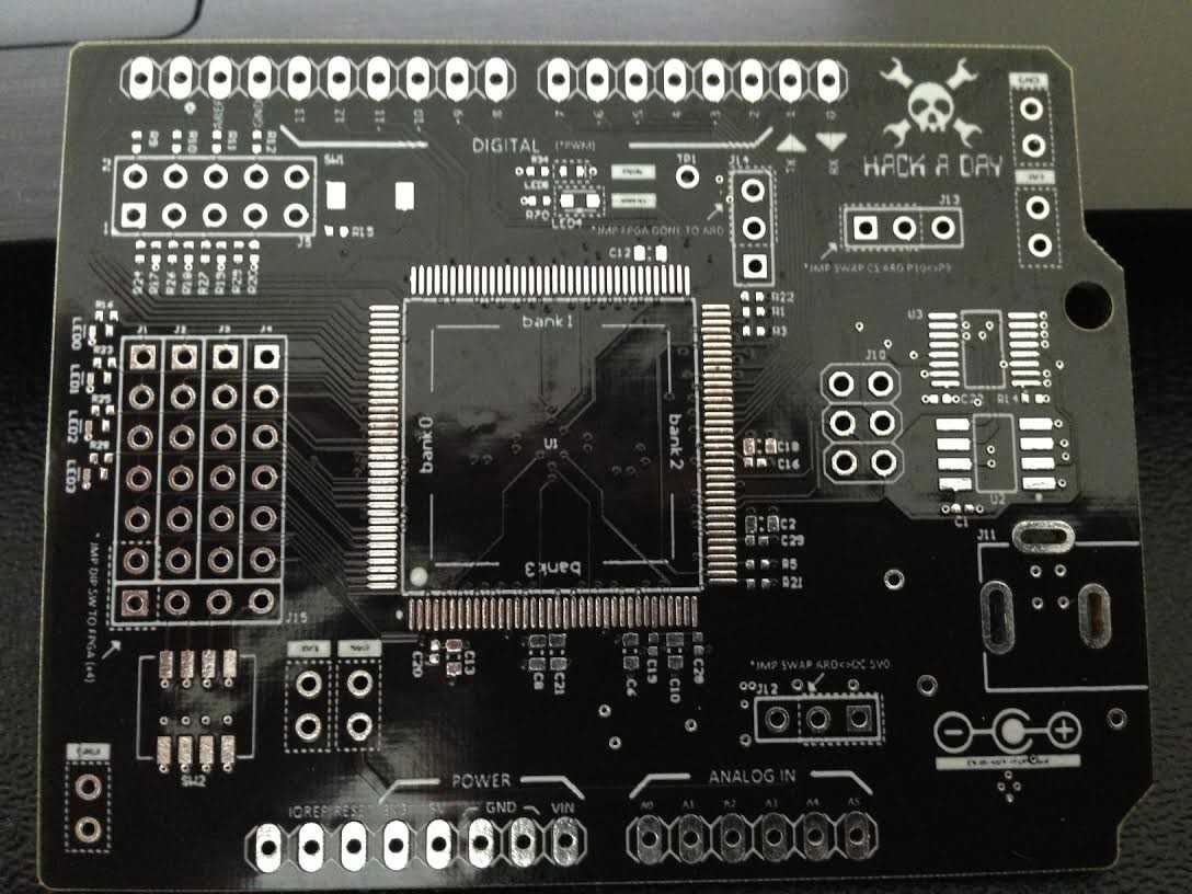
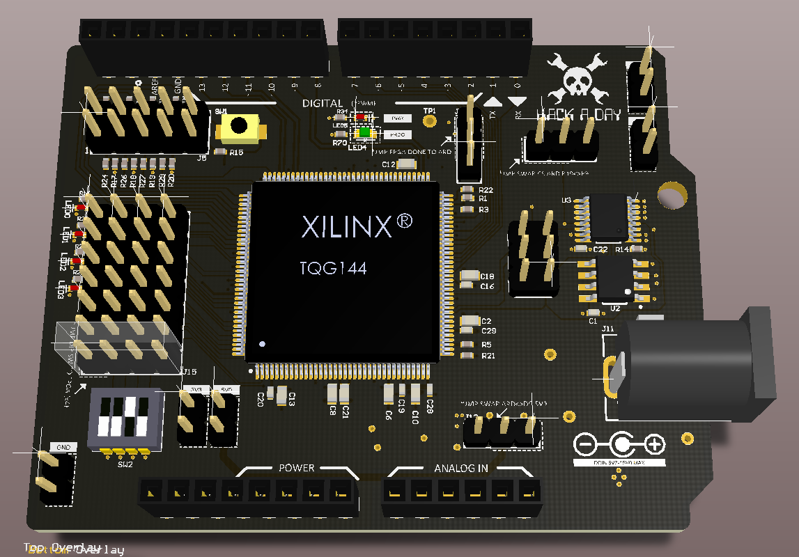
Intending to keep this as compact as possible I'm looking at BGA packages for SRAM and std package for the SPI Flash.  The several that I've chosen will enable me to keep costs below $30 for the whole board (target = $25) and still have head room to do some really impressive stuff with it.  Likewise, this makes a sizeable "prototype area" available to fill with either additional connectors or PTH pads.

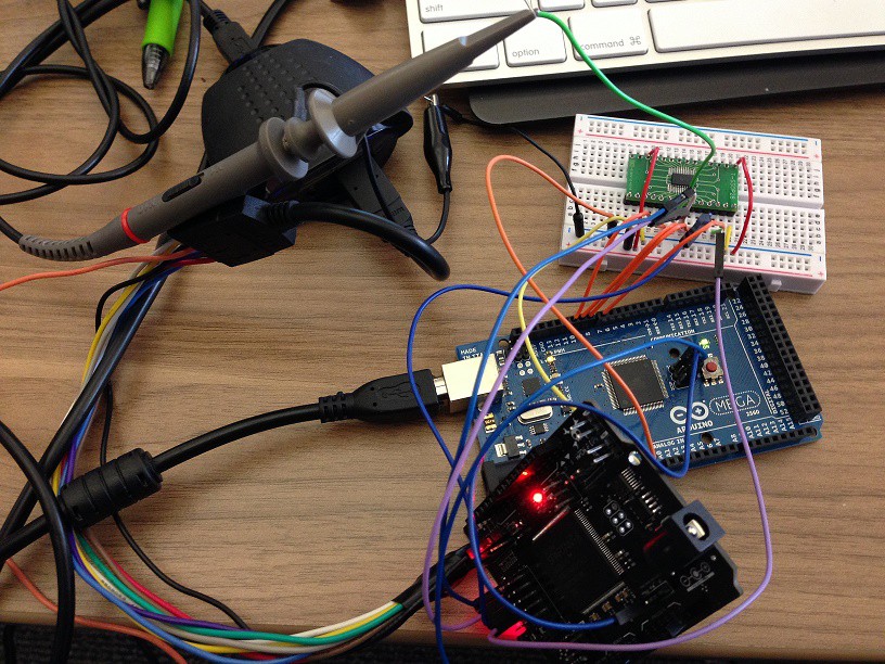
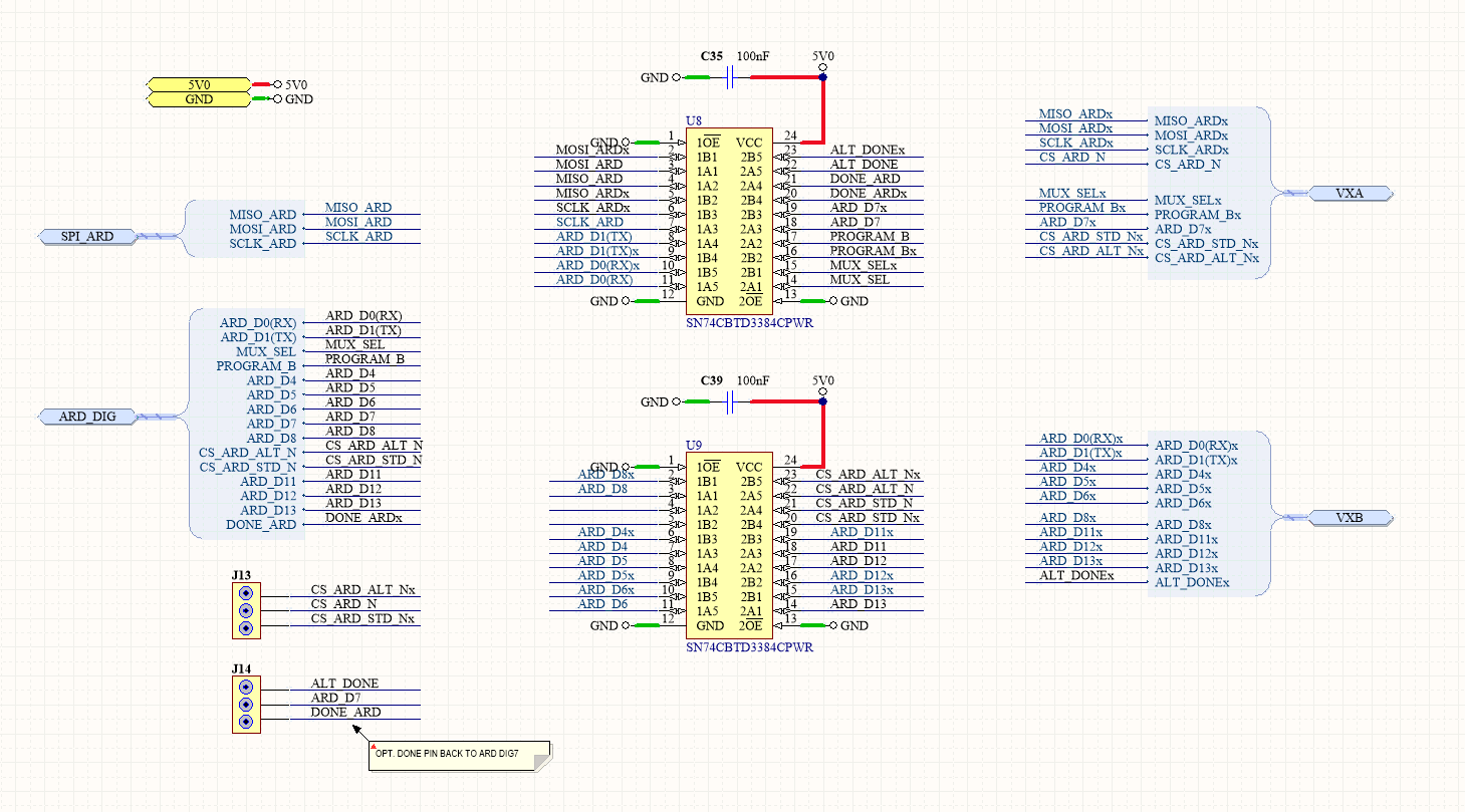
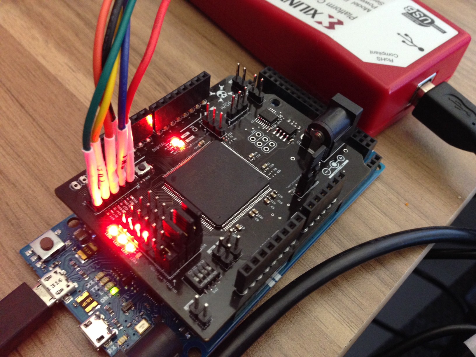
Programming of the SPI flash from Arduino is done via the ICSP header which carries thru to the "daughter" card.  Likewise, I've included a second chipselect (GPIO) to enable the ICSP to connect to the FPGA via SPI (were you to use an SPI slave core in the FPGA to drive FPGA functions...more on this in my next project ;)

Flash is meant to be large enough to be used by an FPGA processor in case someone wanted to use one, and also hold multiple images of the FPGA configuration if someone intends to make this harder to "brick".

Power is still undefined but relatively trivial.  Power supply will offer a few different rails and LEDs and line drivers will be used to provide some visual feedback of programming state and activity.

Git project -- https://github.com/sfgit/FPGA_Arduino_Shield.git

  • 1 × XC6SLX9-2TQG144C Xilinx Spartan 6 LX9 FPGA - Device Playground
  • 1 × S25FL216K0PMFI041 Spansion 16K flash - to hold FPGA configuration
  • 1 × SN74CBTLV3257DBQR SPI Multiplexer - manages access to flash from multiple SPI sources
  • 1 × KC5032A20.0000CM0E00 Kyocera 20MHz CMOS Oscillator - FPGA clock source
  • 1 × IS61WV12816DBLL-10BLI ISSI SRAM - 128Kx16 Asynchronous

  • Uploaded new files to Github

    technolomaniac07/09/2015 at 06:32 0 comments

    Made a few minor cosmetic tweaks, did some stuff on the PCB to try and make the next pass easier to add more IO (something that's been asked for) and really dialed in the output generators and outputs directory. Overall a nice cleanup prior to the latest round of fab. Boards are in the pipeline for mfg and will be 'in stock' very soon again! Check out the github repo. Also planning on changing the licensing to MIT so should make it much easier for folks interested in using this in their own products. Much of this can now be reused for my iCE40 design which is underway and after a 12-hour flight from SZ, I have only a little left to finish to make a second FPGA board, this time using the lattice parts. Altera to follow.

  • Uploaded first how-to video...Walkthru

    technolomaniac12/11/2014 at 07:10 1 comment

    Just uploaded my first video on actually using the board. There are a few others to follow. The video is found on Youtube:

    This describes the various interfaces, the use of the resources, the jumper settings, power supply, etc.

    I have also uploaded the first "Blinking LEDs" example for use with the Xilinx software, available on Github.

  • More FPGA Boards Back & Working!

    technolomaniac10/28/2014 at 23:27 3 comments

    Whew! Last round of mods were huge because as you come to find out quickly, anytime you add a level translator to a board - much less two & much less 10 channels each - you end up having to reroute most of the PCB layout. And as though that wasn't enough, I decided to make a bunch of other small updates and signaling fixes / improvements such that board (a) is now meaningfully different from board (b). <Shudders>

    Still, today the box of boards came back - first time populated by someone other than me - and they look and (more importantly work) awesome. The board shop this time took their sweet time but the wait was worth the cost (almost 10:1 versus US companies for the same quote).

    A few more small tests and it's away they go to the store to be sold! :)

  • Level Translation Mods

    technolomaniac10/01/2014 at 23:57 0 comments

    The first pass of this board was built with the Due in mind (3V3) and other development boards that I had sitting around, almost all of which *other* than Arduino were 3.3V.   In planning the evolution of this however, it quickly made sense to include support for other 5V devices such as the Uno and other Arduino boards.  So I have gone ahead and added a Level Translation circuit and respun the board now with some level translators that will convert the Arduino's 5V0 outputs to a nice, user-friendly 3V3 signal for the FPGA.  This'll ensure support for the Uno and other Arduino's not using 3V3 IO voltages.  Likewise, I made a few other small improvements and fixed a few snags that deserved some attention.  

    Testing the level translator on a breadboard...

    Schematic for the level translation circuit...

    Above is the schematic (new files will be uploaded to github shortly) for the level translator and because the layout needed to change pretty substantially to accommodate these two new devices, the boards went back to fab and are going thru proper assembly at the moment.  

    The part used for level translation is the SN74CBTD3384.  It's a 24-pin TSSOP and it's relatively small, cheap, and performs pretty well with very low series resistance.  Designed for performance up to about 10 MHz and provides  a nice interface to the arduino UNO and other 5V0 devices.  

  • Glamour shots

    technolomaniac09/04/2014 at 00:33 1 comment

    Nothing really to add here except a few simple glamour shots to show how things ended up.  Connected, in this case, to a Due just for fun.  

  • building a (budget) box I'd be happy to open

    technolomaniac08/24/2014 at 20:47 0 comments

    Recently I'd gotten a fair bit of interest from folks wanting to buy or or trade for one of these FPGA boards...And I must admit, I'm not terribly capitalistic when it comes to stuff I build outside of the work context (I often find I just end up giving stuff away, rather than trying to profit on them).  Still, I feel that generally everything I build is a reflection / measure of me and my interests and passions and enthusiasm and as a result, I hate to "ship" junk.  And I hate to own junk!  Better put: I want things to look pro, even if they're outside of the professional context (things move slower, but they just tend to be more 'agreeable' all-round).   

    So when it came time to come up with boxes to ship to folks, I thought I'd spend a little time trying to get this right.  And though I began by getting it wrong - all wrong - I managed to recover nicely I think and these express the 'spirit' of this board in a way that makes me comfortable sending it to my mates / others I've come to know thru electronics / n'er-do-well hackers, what-not.

    So the first order of boxes arrived an candidly, they sucked.  Corrugated die cut, white on one side, natural on the other.  The white is faded, poorly applied, the folds are not crisp and clean, the slots look to have been cut far to large for the flap thickness (makes the boxes loose along the edges) and the overall accuracy is rubbish.  I'm embarrassed for the USA stamp they bothered to apply to a crap box.   You can see the thin paper over the corrugation making them weak and hard to managed without some serious tape / glue.  Have a look:

    *****

    **Still, I tried to "make-do" (if I find myself using this expression, it is undoubtedly a reflection of frustration and poor judgement more than anything else)

    ***

    ***Ok, complete rubbish.  I will NOT send this off to a friend.  It's totally unacceptable (I'm that guy that puts stickers in a box along with your xmas present...details!).  So I packed it in and I pinged my good friends at Uline.  They are pro.  They do boxes.  All sorts of boxes.  And they do them well.  

    What I got was a far superior product.  Well cut, sturdy,  and although slightly larger (4x4" vs 3x3") there is clearly a far better process afoot here than at the first place I used.  Still die cut but looks to been done with better materials, better equipment, and the sort of love I like to see. Have a look:

    ***

    ***Now that I had a better box, I still didn't have an awesome one.  I had something nice, solid, more precise, but I wanted awesomeness.  Maybe not apple's barely-air-gets-through precision (impossible to do in my house on a budget) but something that at least looked cool and that I might keep after I took the board out and use for knickknacks like jumpers or those extra header bits or such.  Nice to pack away that arduino or flying leads and have some room for the USB cable and what-not.  

    So I go my thinking cap on and thought to use the Hackaday logo on the outside of the box.

    First I tried some die-cut stickers...

    ***

    ***

    Nah, fail.  Nice and all, but too much contrast, not enough of a story in there.  

    This is a board for people who want to build whacky shit with FPGAs and it should reflect that.  I couldn't have a clean edge, precision cut sticker on the box.  (Inside maybe)  I needed something that also complemented the rough edges of the imperfect box.  So I just happened to be sitting in my office and inspired by a pic of graffiti that serves as my desktop background, I decided to use spraypaint.  

    (Think: sweet road crew awesomness...what better to have in your gearbag than an FPGA board?)  

    ...But with what image?  Why the Hackaday logo of course!  (thank you to the die cut sticker that served as my cheap stencil)

    ***

    Tag that thing...

    ***

    ***

    ***The lineup...

    ***

    ***Something I'd keep on my desk......

    Read more »

  • Ding ding...Round 2 - New board look purty

    technolomaniac07/17/2014 at 17:50 0 comments

    Got the new boards back from Advanced Circuits (they rock BTW...attention to detail like few others) and they look awesome.  Went with black soldermask this time around and it makes things look so much cooler (much more Hackaday-chic).  These boards have a few new details including dipswitches (bloody small!), LEDs, a few extra test points, tented vias (BGA Soldering loves tented vias!) and a few other cosmetic tweaks esp. to the silkscreen.  The first batch worked fine so hoping this works without issue as well.  

  • Parts arrive for first 50p run!

    technolomaniac07/16/2014 at 17:15 0 comments

    Got enough parts to build 50 boards today.  Updated stencils arrived, woo hoo!  Retreating into soldering dungeon to spin up one or two to verify all's well with the world.  

  • Board goes 3D - like *really* 3D

    technolomaniac07/15/2014 at 22:40 0 comments

    Added step models to all of the interesting parts of the board to make things look and feel more authentic and to size up enclosures and such that I will release that you can easily 3D print.  Have a look at the pic below in the project overview.

  • New Design Files Uploaded To Git

    technolomaniac07/04/2014 at 07:57 0 comments

    Uploaded a new batch of design files including PDFs to github.  The repository can be found here and this rev contains some nice functional improvements.  See previous project log for some details and see git log for summary of changes.  This will be the final few changes before I build a reasonable qty of these boards (~100).  If anyone's keen to own one, let me know...I have the BOM down pretty low now and be a nice addition to the tool chest.  

View all 35 project logs

  • 1
    Step 1

    Step 1 - Don't panic.

  • 2
    Step 2

    Step 2 - Import the Arduino board file into Altium Designer:  Using Altium Designer (AD) requires that I import Eagle board into AD.  AD14.x includes an Eagle importer.  Used source files from the Arduino site to import in AD.  

  • 3
    Step 3

    Step 3 - Build major footprints:  Costing the available board area requires building the major footprints and placing them on the PCB.  Built early footprints and placed to determine what additional space is avail.  Files in git.

View all 11 instructions

Enjoy this project?

Share

Discussions

hackhead79 wrote 03/30/2014 at 01:17 point
I am still in the beginning stages of being a maker (just made my dive into the Arduino world with an Arduino Mega 2560 ) but reading about FPGAs seriously tickles my maker bone. I would love to learn how to use FPGAs (including learning VHDL). Especially after buying a 5" display for my Pi for about 5€ and realising it needs an FPGA/CPLD controller to work.
So by the time your board is ready, I would be very glad to use your board as my first FPGA/VHDL -learning platform!

  Are you sure? yes | no

technolomaniac wrote 04/02/2014 at 05:20 point
Awesome to hear. And I'm preparing a series of videos on FPGA basics. The concepts, like anything, take a little effort, but after you nail the basics it's relatively straight-forward. I'll have some boards for cost once this is all said and done (design is actually further than what I've documented so far) so if you'd like one, drop me a line and I can give you a BOM cost and assembly and such and share a "kit" or a completed board. The only real beasts to solder are the super small QFN packages. With solder paste and an oven or hot air, it's all within reach.

  Are you sure? yes | no

hackhead79 wrote 04/02/2014 at 19:24 point
That sounds awesome! Yeah, it would be cool if you could send me the BOM for a kit or similar!
I read a 65-page VHDL primer a few days ago of which I understood a pretty good deal (I have some light to moderate previous programming experience) and it really seems manageable, very logical and much clearer than C[++] and the likes. I really like that processes can be timed very accurately and that multiple processes can run in a truly parallel fashion.

From what I've seen on Youtube, small pitch SMD soldering does not look like rocket science but I might be wrong ;). I'll try my hand a these small footprints in a few days on a DIY CPLD board when the components arrive. (I'll start a project here on hackaday projects about it in a few minutes - the board is built with a Xilinx XC9536XL but has only about a tenth the amount of logic units your board will bring, i.e. 800 logic gates, 36 Macrocells compared to 9152 the Spartan 6 XL9 has!).

Sooner or later I want to upgrade to FPGA anyhow, so it would be really cool to assemble and bring to use one of your FPGA boards so BOM / cost for a kit or similar sounds great. And I am looking forward to your video series to learn more about FPGA programming!

  Are you sure? yes | no

mkr506 wrote 03/14/2014 at 16:51 point
Thanks, this .. is.. Great! i'm a second year student at uni (york UK ... Woo!) and this is a perfect project since its holiday time, i've now been introduced to vhdl (and the joy that is Xilinx software) -and i'm also totally skint!!! Thanks for all the future stuff

  Are you sure? yes | no

technolomaniac wrote 03/14/2014 at 17:51 point
Awesome! I'll keep posting updates however if you're keen to test a prototype, pm me on twitter @technolomaniac and after I spin them up, I'd be happy to try and ship you one.

  Are you sure? yes | no

DubStation Freeside wrote 03/13/2014 at 12:50 point
KUDOS. This could be a really awesome thing. I know we'll be playing with them asap.
Considering the fact that stuxnet is still probably floating around, I predict much dark humor surrounding said shields.

  Are you sure? yes | no

technolomaniac wrote 03/13/2014 at 17:04 point
Ha! Indeed. This certainly has "dark potential". Was thinking it'd make a fun way to introduce people to bitcoin mining as well. There's heaps of those cores out there and they are a good lesson in the virtues of FPGAs and how their resources differ from an OTS CPU.

  Are you sure? yes | no

Eric Evenchick wrote 03/05/2014 at 16:03 point
Seems like a great, cheap way to get into FPGAs and HDL. I can imagine a ton of ways to use the Arduino and available shields for communication, and use the FPGA for heavy lifting.

  Are you sure? yes | no

technolomaniac wrote 02/03/2014 at 22:11 point
Added some content to new git repo for this project. Nothing too fancy yet, just costing the board area versus component sizes. See here: https://github.com/sfgit/FPGA_Arduino_Shield/

  Are you sure? yes | no

Similar Projects

Does this project spark your interest?

Become a member to follow this project and never miss any updates