0%
0%
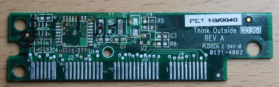
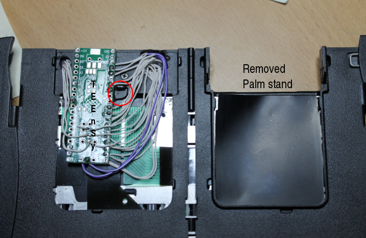
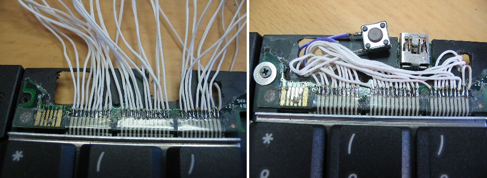
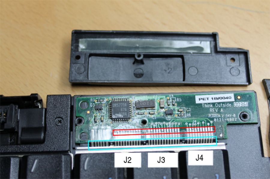
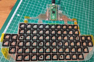
convert Palm foldable keyboard to USB
from my Palm Pilot days I have some of those foldable keyboards lying around and try to find a way making them usable via USB
 mclien
Become a Hackaday.io member
Already have an account? Log in.
Just one more thing
To make the experience fit your profile, pick a username and tell us what interests you.
Pick an awesome username
hackaday.io/
Your profile's URL: hackaday.io/username. Max 25 alphanumeric characters.
Pick a few interests
Projects that share your interests
People that share your interests


 Kārlis
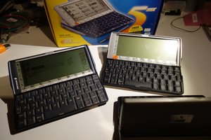
 RasmusB
 mr. mosby
Stumbled across this while researching trying to bluetooth a couple of old palm k/bs. Can't stand/use the modern small portable keyboards - I've got big fingers.
Like you I don't really want to have lots of add-on plugins to cart around.
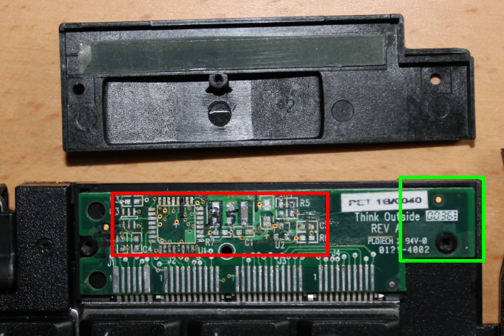
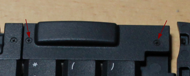
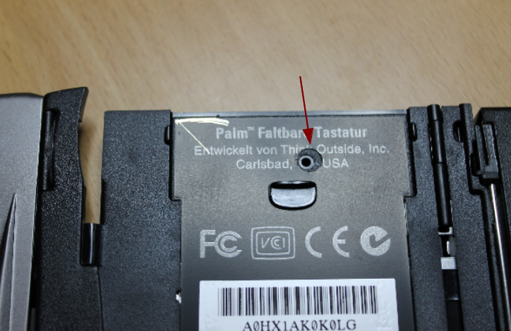
Maybe I'm being too timid, but how did you get into that compartment with circuitry without damaging the compartment lid?
On mine having undone the screws the top stays in and I'm guessing there's a one time plastic peg on the "lid" to hold it sealed, probably what looks like a plastic foot on the rear of that section.
Same Q for the side with the rest. While I have a spare I'd rather get two usable k/bs than one and a few spare pieces.
On a completely different question has anyone ever seen these with a UK keyboard layout (or at least keys with UK keyboard combos such as 2 & ", 3 & £ and @ & '