 mclien
I removed all components from the original PCB to get a good scan from it and to find out wher and how much space is there to place components there.
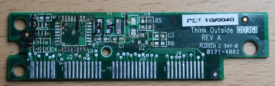
It's about 65 to 20 mm in square. (exact measurements and scan to follow).
And here the same with the top cover flipped:
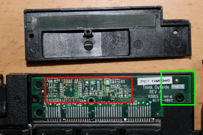
The board was populated on side only. The reason is the backside is lying nearly compleedly tight to the plastic housing with the only exeption beeing the part in the green marked area, where aspace of about 2mm is beneth the board.
the red marked area is where the components where paleced/ could be placed. There is a max of 3.5 mm in hight in the middle area, slping down to 2.5mm to both sides (to upperpart is what goes on top of the board.
The foodprint of the U1 is 7mm square for the housing, which is the sice of the QFN foodprint of the atmega32u4 chip, which is my faveroed chip for this poject because it has USB on board and is arduino compatible, so it could be used as mc itself or could be flashed with the arduino bootloader.
I'm currently thinking of double using this PCB for an USB -thinkpad keyboard adaptor, too. This would mean to place the according socket for those keyboards additionally onto the board, what will result in some space issues.
I can think of some solutions to this:
A) place all components for the palm keyboard inside the red area and the thinpad socket on the other side of the PCB and leave it unpopulated for the palm use. Will need to track 2 paths for the populating, but simple enough since it's just dropping a part.
B) place the little SMD parts, the thinkpad socket and the USB socket inside the red area and the atmeag on the other side of the PCB. Would require cutting a hole into the case where the atmega will rest in. This would give most space for routing the PCB, I'd think.
C) mostly ike B) but placing the atmega on the backside of the PCB fitting inside the spare gap in the green marked area. Most likely will give too little space for routing.
There is also the idea of having alle pins routed to standard plug connectors (like the ones at the arduino shields), most likely as option for debugging and not fitting inside the housing.
Discussions
Become a Hackaday.io Member
Create an account to leave a comment. Already have an account? Log In.