0%
0%
Digital Holga
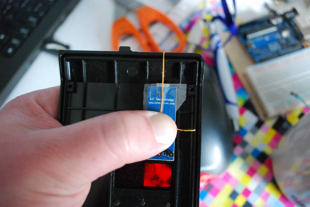
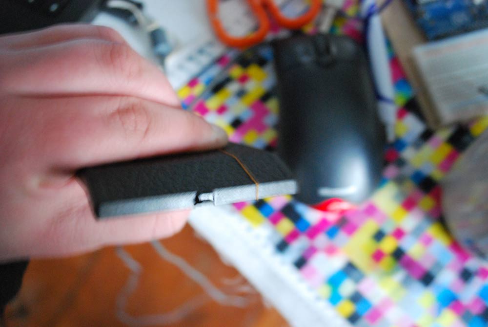
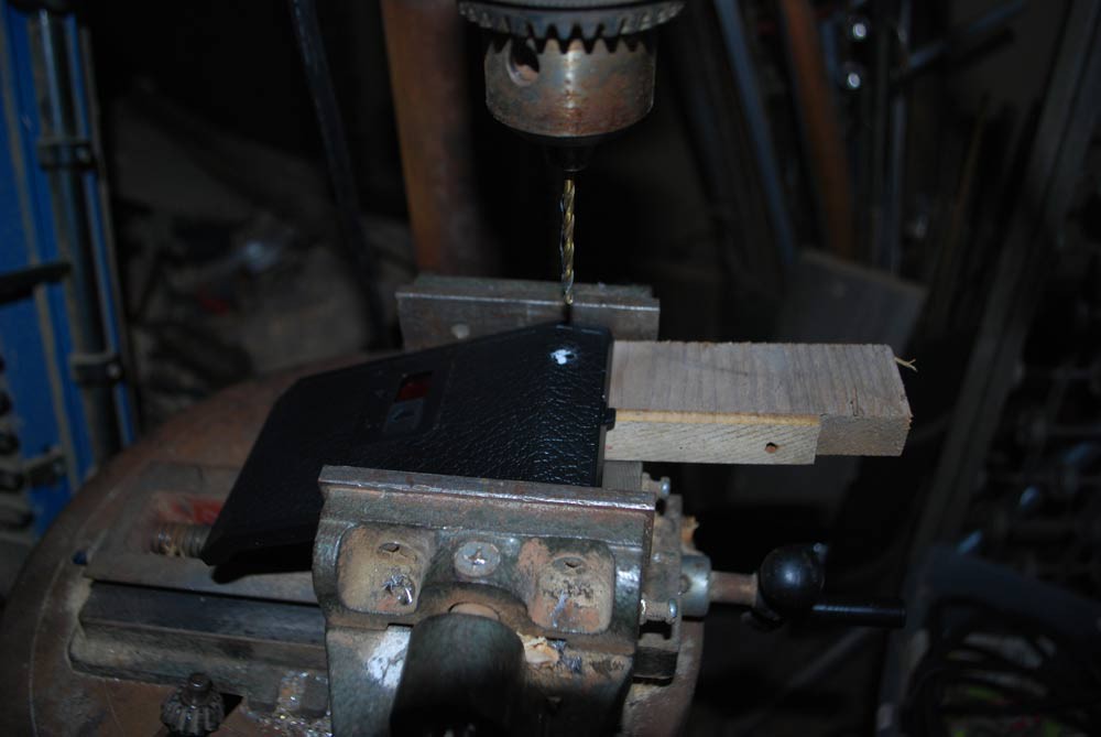
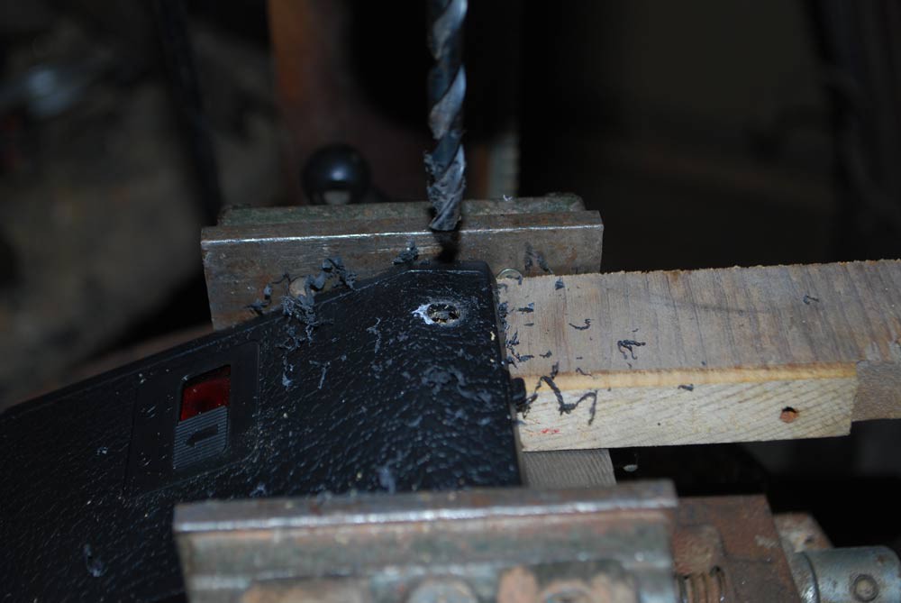
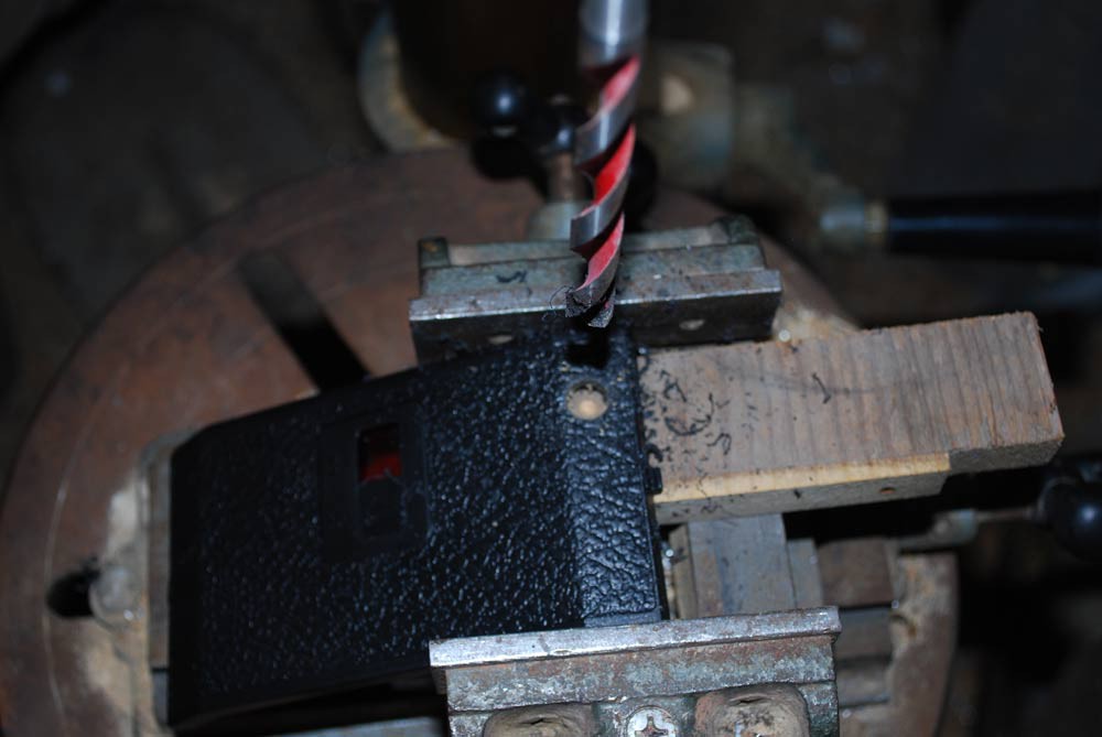
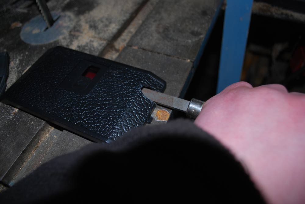
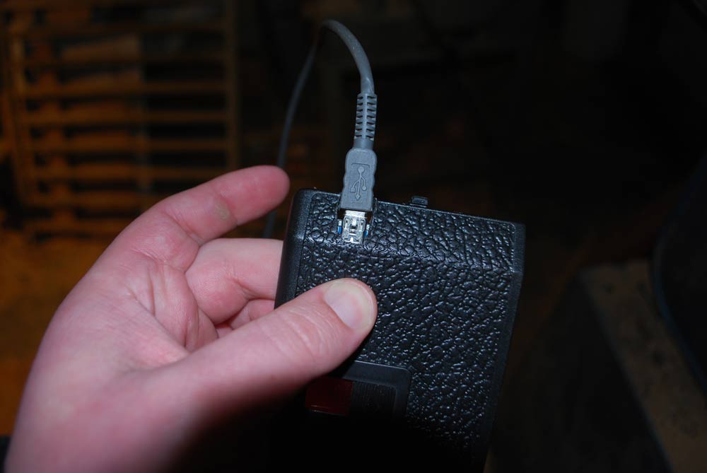
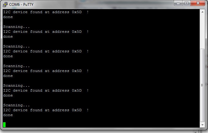
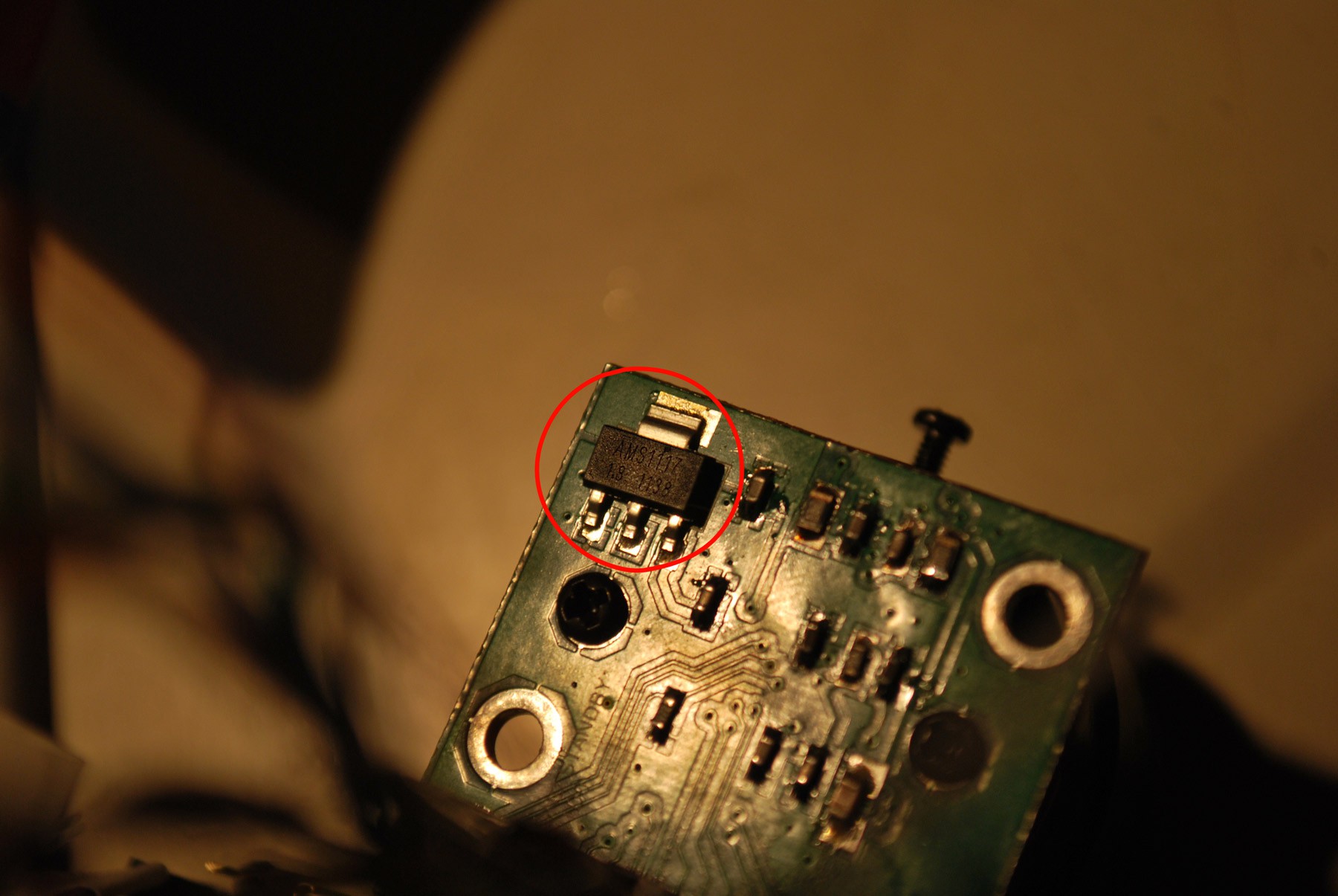
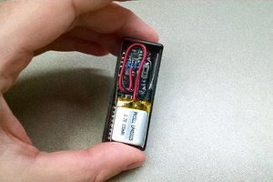
Conversion of a Holga 120S to digital format with SD card output.
 Anthony
Become a Hackaday.io member
Already have an account? Log in.
Just one more thing
To make the experience fit your profile, pick a username and tell us what interests you.
Pick an awesome username
hackaday.io/
Your profile's URL: hackaday.io/username. Max 25 alphanumeric characters.
Pick a few interests
Projects that share your interests
People that share your interests
nT!1TIBRsFSDhukw~~60_12.JPG)
 Eric Herbers
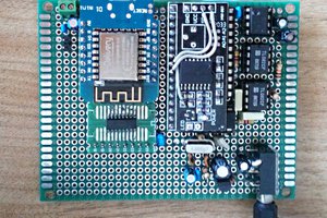
 Emilio P.G. Ficara
 Just Me NL
 SouthMade