 ccates
Prostar 16x16 Panel Reverse Engineering - The buffers and the CMD signals

Next I looked at the basic structure of the six buffer ICs (Yellow).
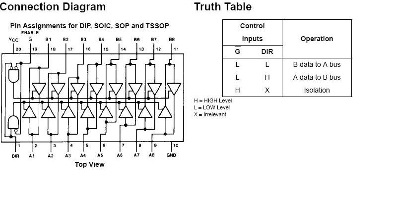
I thought initially that the Enables on the buffers were being used to control "banks" of the drivers. Upon using the meter, however, I found that all of the active low Enable lines were tied to ground and all of the DIR inputs were tied high. This meant that all of the buffers were acting as simple 8 bit non-inverting buffers. No control inputs, no bi-directional nonsense - They are just here to bump up the current. More lovely simplicity.
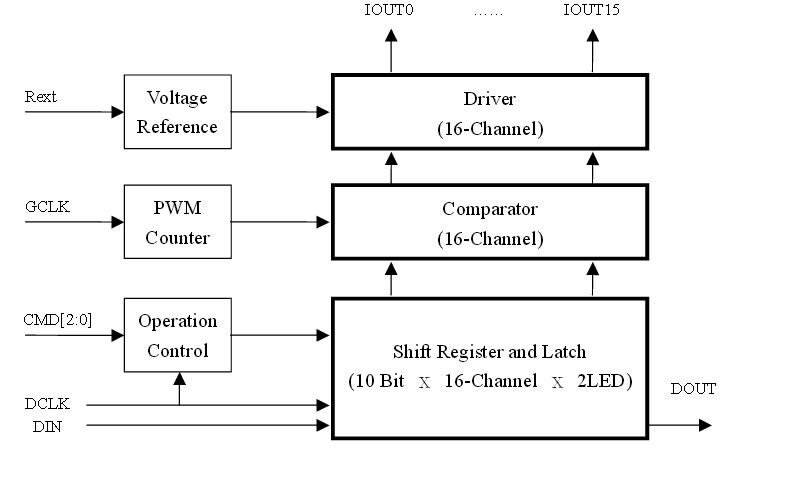
In order to continue it is necessary to understand how the driver controls the LEDs. As shown in the datasheets the driver has three main components for each LED output - a controller/shift register and latch, a pwm counter/comparator and a set of output drivers. When the shift-in command is issued the Dclk input is used to clock the data into the shift registers for the 16 LEDs. Each LED requires 10 bits of luminance data. When the buffers for all of the LEDs on the chip are full (160 bits worth) the capture command is issued which latches the data into the shift register where it drives the inputs of the comparators. The driver turns on the LEDs and each LED's pwm counter starts to count down using the GCLK signal as a clock. When the comparator sees that the pwm counter has reached zero the LED is turned off. When done repeatedly with the emitting command, this controls duty cycle and thus the brightness of the LEDs.
I decided to see where the control inputs were coming from on the driver ICs. Each chip has three control lines: CMD0, CMD1 and CMD2. These lines are used to control the mode of the chip, when it is clocking in data and when it disables and enables the output. The control codes are:
CMD
Bit2 Bit1 Bit0
0 0 0 - Mode 1 - 16 LED MODE
0 0 1 - Mode 2 - 32 LED MODE - not used in this panel.
0 1 0 - Shift-IN
0 1 1 Capture
1 0 0 - 1st LED emitting
1 0 1 - 2nd LED emitting - not used in this panel.
1 1 0 - LED disable
1 1 1 - Test Mode
Upon much beeping of my meter and a considerable amount of time I then discovered that all of the CMD signals (0,1,2) on all of the driver chips were coming from two places - The buffer chips marked U13 and U22. Tracing them back shows that CMD 0 comes from pins 14 - 17 of U13, CMD 1 comes from pins 11 - 14 of U22 and CMD 2 comes from pins 15 - 18 of U22. On the other side of these buffers the corresponding inputs for each signal are tied together - that is all of the CMD0 inputs are tied together, all of the CMD1 inputs are tied together and the same for CMD2. The CMD 0 buffer inputs then go back to pin 20 on the input connector, the CMD 1 inputs go back to input connector pin 17 and the CMD 2 comes from input connector pin 16. Thus the buffers U13 and U22 generate the CMD signals for all of the driver chips and only one set of CMD signals drives the whole board. Cool.
Next up - The clock signals - DCLK and GCLK
Discussions
Become a Hackaday.io Member
Create an account to leave a comment. Already have an account? Log In.