 ccates
 Feb. 9, 2015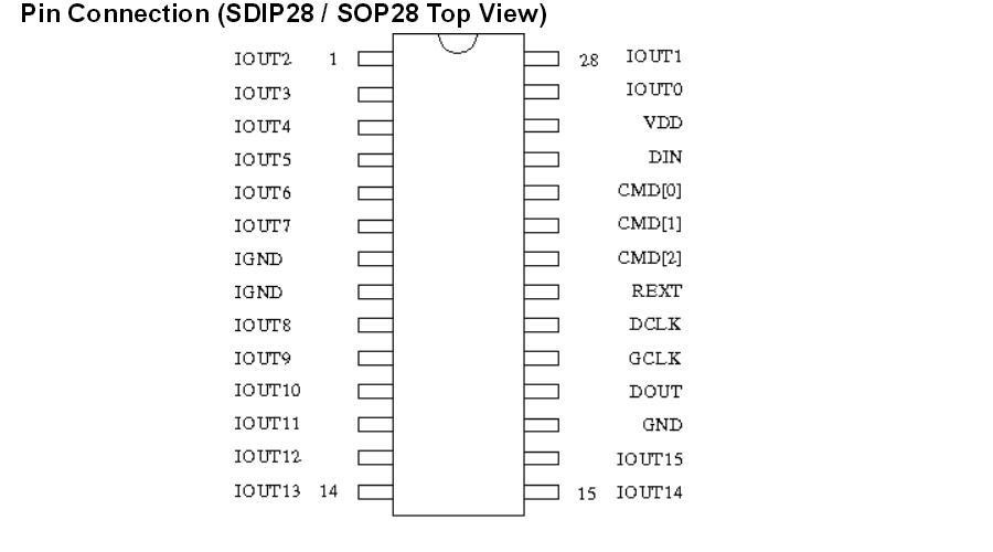 The Clocks - GCLK and DCLK
Now that we have looked at the CMD structure used to relay the CMD signals from the Input connector to the driver chips I wanted to see how the chips got the DCLK and GCLK signals and determine where thes signals came from.
From the data sheet we know that the GCLK is the clock that determines the rate at which the luminance data gets counted down to zero in the PWM counter. The rate at which the countdown occurs is very important - it determines the on time in the PWM duty cycle and thus the brightness of the LED. Since the LED can be on for 1024 GCLKs max per cycle the GCLK must run at at least 1024 x minimum flicker frequency of 70 to 90 HZ or 70000 to 90000 HZ. In reality some flicker in this type of display is acceptable since it is rarely viewed for a long period of time thus the GCLK can be run at a much lower frequency.
The DCLK is the clock that is used to get the data clocked into the Luminance shift registers. The data is clocked in serially - one bit at a time. The DCLK signal frequency is determined by the rate that we want data to be changed and the size of the display. Each LED takes 10 bits of luminance data per frame. There are 768 LEDs on the panel yielding a total number of bits per frame of 7680. If we want to change the frame 10 times a second for animation purposes we must clock the data in at 76,800 bits per second. If we want full video at 60 hz then we need a DCLK frequency of 460,800 bits per second. Since the data sheet says that the MAX DCLK frequency is 15MHZ and MAX GCLK is 20 MHZ it appears that the chips are well able to handle full video.
I have doubts that a Arduino can handle it though. Oh well, we'll see how far we can push one later. I'll be happy if I can get several frames per second.
So how do the GCLK and the DCLK get to the chips? Turns out both the GCLK and the DCLK path is somewhat simple. It uses a buffer cascade similar to the CMD signals. The GCLK inputs on the chips are tied together in 8 banks of 2 vertically adjacent RGB groups.
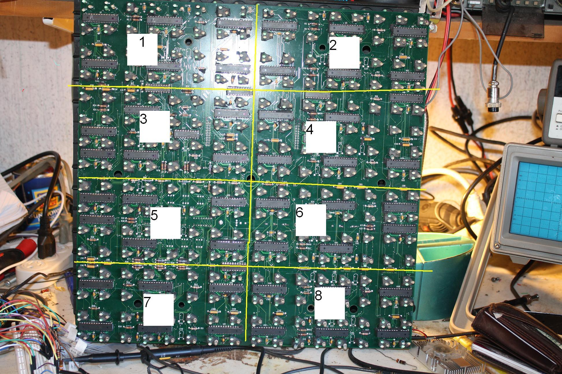
The GCLKs of the six chips in these banks are tied together and sent to one output each of either U14 or U42. U14 has outputs for banks 1 - 4 and U42 has the outputs for banks 5 - 8. The inputs of U14 and U42 go back to pin 14 of the input connector. Thus all GCLK inputs are buffered from input pin 14. The DCLKs follow a similar pattern - all of the driver's DCLK inputs are simply buffered signals from input pin 18. It took quite some time to beep this all out but in the end it turned out quite simple - send a DCLK and a GCLK signal into the input connector and it ends up on all of the chips.
This leaves up with just one set of signals in - The Data in or DIN signals. They turn out to be a little more complicated as we will see in the next entry.
Discussions
Become a Hackaday.io Member
Create an account to leave a comment. Already have an account? Log In.