 Bud Bennett
Two years ago I did not think that anybody really needed 6S LiPo batteries. Now they're everywhere. So I decided to capitulate and build a magnetic switch that would accommodate the new technology. I have a friend, not an engineer, that keeps insisting that 5S LiPo with a 40A or 50A ESC is the way to go for his latest high speed demon airplane. And I have watched as the smoke pours from the cockpit as he destroys his latest high dollar brushless motor.
The Schematic:
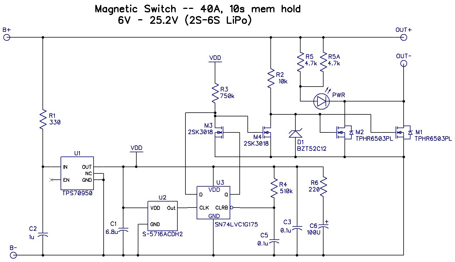
Not much is different. The change is to the FETs and how they are driven. Previous magnetic switches were driven with 5V gate voltage. This circuit level shifts the gate voltage of the output switching FETs to 12V to extract every bit of RDSon that the FET is capable of providing.
I searched Digikey for the FETs that would offer sub-mΩ RDSon with logic level gate voltages. Yes, I could find them, but there was always a 50% improvement when the gates were driven by 10V. A 6S LiPo battery offers 25V, so the extra gate voltage is not difficult to come by. The best FET that i could find for this application was Toshiba's TPHR6503PL -- about $1.40/each from Digikey in low quantities. It can withstand 30V (VDS) with an RDSon < 0.65mΩ if driven with VGS > 10V. Two of them in parallel should provide < 0.38mΩ. But these FETs are not the wimpy 3mm x 3mm powerPAK devices...they come in 5mm x 6mm powerPAKs, requiring a lot more PCB area. This is not a bad thing -- the more PCB area the lower the theta-jA ( the junction-to-ambient coefficient). I also figure that any plane requiring 40A/6S will have a reasonably large canopy volume to safely install this switch.
In order to get the reduced RDSon from the TPHR6503 I added M4, R2 and D1. The gates of M1-M2 are now driven to 12V when the magnetic switch is activated. The PCB dimensions increased to 16mm x 22.7mm. Still pretty small by most standards. In fact, it should be larger to withstand the increased power dissipation. The layout has components on both sides.
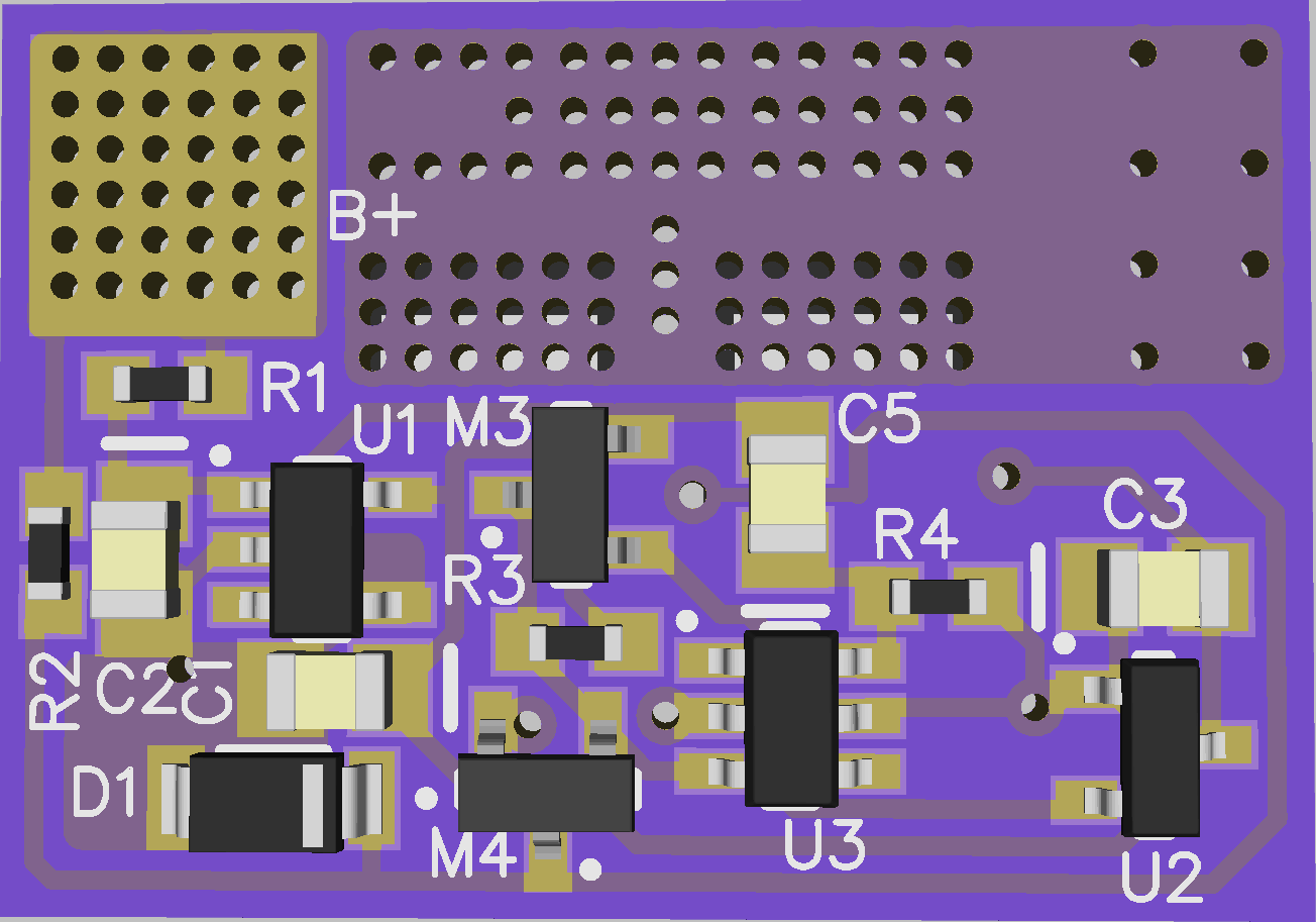
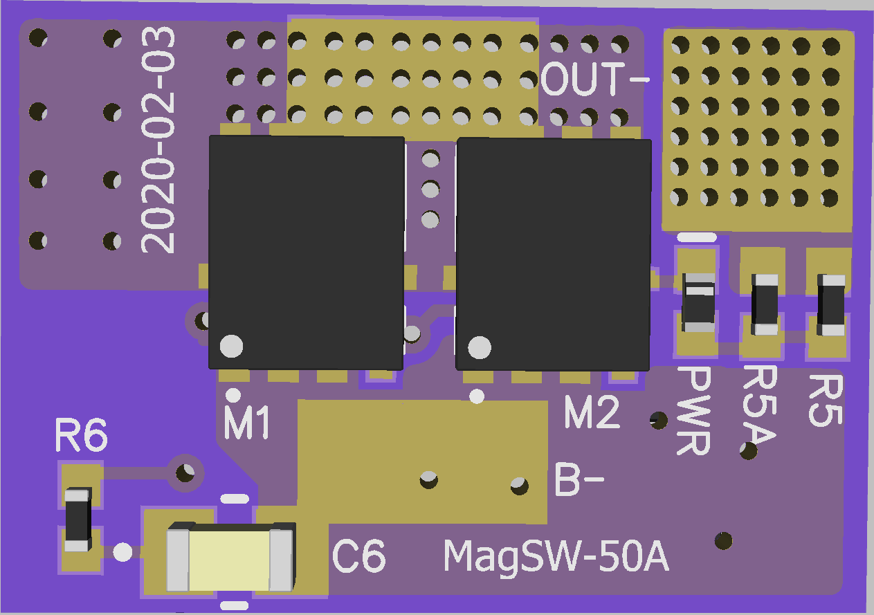
Most of the extra area is for the larger area required by M1 and M2. I added space between U2, the Hall effect switch, and the high current ground trace -- hoping 3.5mm is adequate distance to prevent the switch from tripping off during high current events. If that doesn't work, then the Hall effect switch will have to be moved off the board. The landing pads for B+, B-, OUT+ and OUT- are not through hole -- I decided that the large 12-14 AWG stranded wire would undergo a severe 90° bend if forced into a hole, so now the wires are simply soldered to a landing pad. The landing pads will accommodate up to 120mil diameter wire (12 AWG). In addition, there are numerous vias to help spread the heat and conductance between the top and bottom layers. The board will use 2 oz. copper for improved heat dissipation.
The switch should dissipate a maximum of 0.6W for an applied current of 40A. Maximum current can exceed 1000A for short durations ( less than 100µs). That should be adequate.
The PCBs are still small, and therefore inexpensive -- 3 boards are only about $2.80 from OSH Park.
[Edit 2020-02-02: BHarbour pointed out my laziness in his comment. The following is a bit of extra work to solidify the design.]
Reducing the standby current:
I had originally set the value of R2 = 10kΩ. I was sure it would work and did not really consider the impact on standby current. I don't usually leave the battery connected more than 3-4 hours; when the model is returned to its resting place the battery is removed. It would be better if the standby current was low enough that there was no need to disconnect the battery. This can be accomplished by raising the value of R2 to 1MegΩ. (A MegOhm is my personal limit -- enforced by a few years in the automotive industry. High values of resistance are subject to degradation over time by crap that collects on the PCB surface.)
I spent a few minutes with a calculator and LTspice to get feel for what would happen if R2 = 1MegΩ. The simulated circuit is not exact, but close enough:
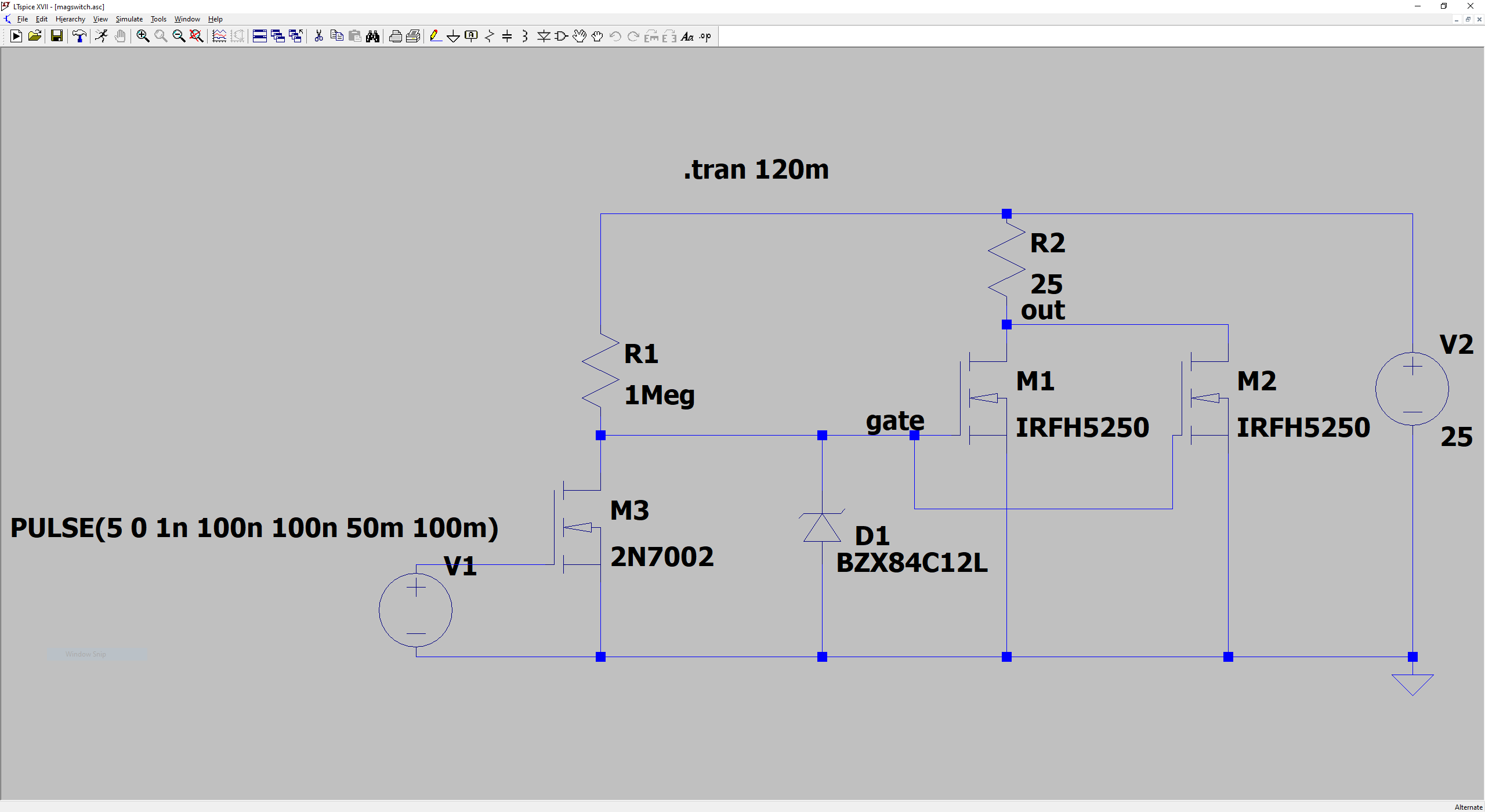
The results align with my expectations after using the calculator. The two big FETs have about 1nF of capacitance from the drain to gate. This is also called Miller capacitance because it gets multiplied by the gain of the FET during the transition of the drain from a high to low voltage in this case. The Miller cap holds the gate at its threshold while the drain moves from 25V to GND, as shown in the simulation.
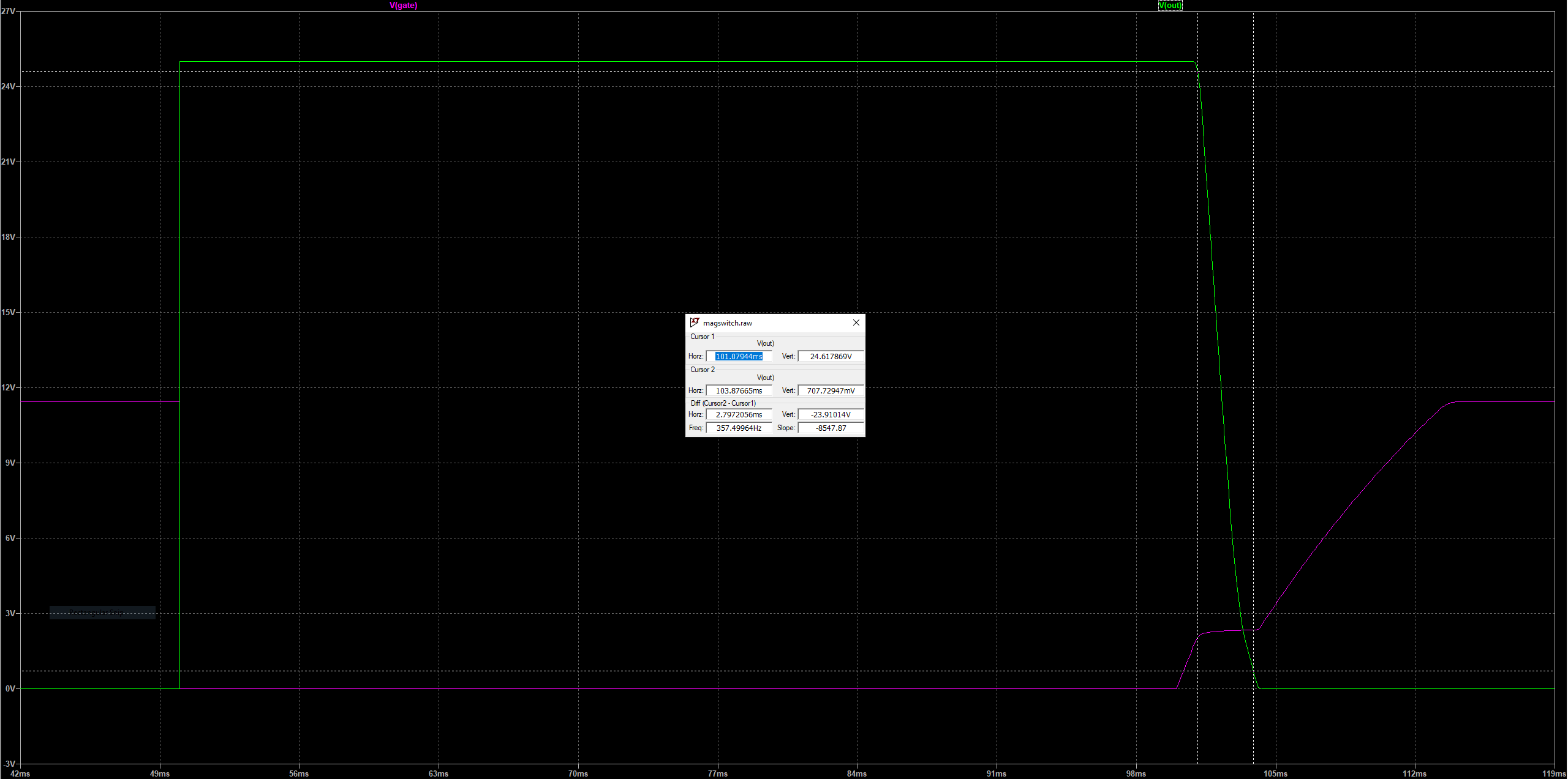
The switch transition is nearly 3ms. I doubt that 3ms will affect the electronics in the receiver or ESC. The Zener diode only achieves ~11.5V due to the low current from R2, but it is plenty for gate drive. I don't really trust the LTspice model for the Zener, but it's a starting point. (It is worth noting that the temperature was 25°C for these simulations and there is a paucity of data for higher temperatures.) I also simulated the circuit with a supply voltage of 6V and 11V: transitions were much slower, but probably still acceptable. I will have to conformally coat the board to prevent contamination from degrading the performance. The schematic was updated in the details section of this project to reflect the new value of R2.
Depopulation:
I will probably build the first prototype with a single TPHR6503PL. This FET has a max RDSon = 0.65mΩ (0.41mΩ typical) @ VGS = 10V. With a load current of 30A, the power dissipation of the single FET will be less than 0.585W. Assuming a theta-jA = 50°C/W, which might be a bit low for this small board, the temperature rise should be less than 30°C. That's not very much for a switch that is controlling 750W of power! Depopulating a FET will save about $1.60.
Discussions
Become a Hackaday.io Member
Create an account to leave a comment. Already have an account? Log In.
Isn't the R2, M4, D2 path going to raise the idle current significantly? When the M1,M2 are off, you have the battery input voltage across a 10K resistor to ground.
Are you sure? yes | no
Yes it will. I figured that the battery would be disconnected within a few hours and the drain would not be a big issue. If I raised R2 to 1MegΩ I'm not sure if there will be enough current to get past the knee of the Zener diode -- but it just has to climb above 10V. Also, the gate rise time increases due to 10nF of input capacitance. I would also have to conformally coat the board to prevent leakage currents (nail polish). With R2 = 1Meg the standby current drops to around 35µA, which would be low enough to just leave the battery connected for extended periods.
I can try the 1MegΩ when I get the boards.
Are you sure? yes | no