 tshen2
in my last update, i assembled a mediocre monitor using an AU Optronics LCD panel. it required an LCD control board to act as an HDMI-to-LVDS converter, for LVDS is the language of most LCD panels.
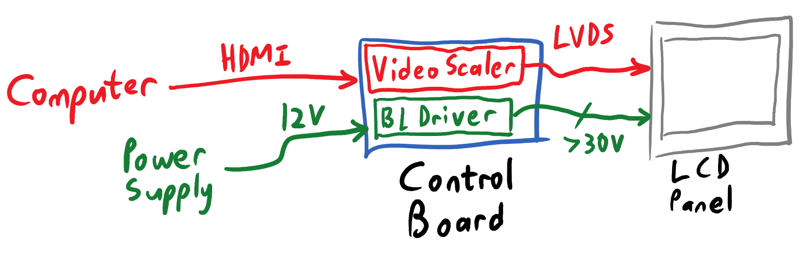
[old-fashioned LCD panel requiring an LVDS converter to connect to a computer.]
but LVDS is losing popularity. as our phones & tablets keep shrinking, how can anyone make room for that LVDS-converter chip? the logical solution is to build a standard ('not LVDS') video interface into the panel, to connect it directly to your graphics card.
the embedded Displayport (eDP) standard was introduced in 2008 to do exactly that. Displayport is the best video interface, LCD manufacturers can build eDP interfaces directly into their panels, and those panels no longer need an LVDS converter.
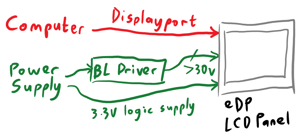
[LCD panel with embedded Displayport. the video interface connects directly to computer's graphics card.]
do note that eDP, while electrically identical to Displayport, does not use the standardized Displayport connector. every manufacturer has their own favorite connector which can vary from panel to panel. this is why all eDP hobby projects boil down to 'how do i connect these super-high-speed RF signals from my Displayport connector to this crazy LCD panel connector?'
Examples:
- Retina iPad panel hack (EmerytHacks)
- Retina iPad panel hack (OSCAR)
- Retina MacBook hack (Rozsnyo)
at this point, since all the cool kids were hacking the 9.7" Retina iPad panel, i decided to do it too. and why not? it's a great (if small) IPS panel with awesome contrast & colors & viewing angles. it's made by LG and the datasheets are everywhere.
so what is actually needed to get it working?
- an electrical connection from a full-sized Displayport jack to the tiny Molex connector which fits the panel's ribbon cable.
- a 3.3V supply voltage to run the panel's logic circuits.
- eight ~20mA bias currents for the LED backlight - this could be as simple as eight current-limiting resistors.
it would have been sensible to build the bare minimum first, and get fancy later.
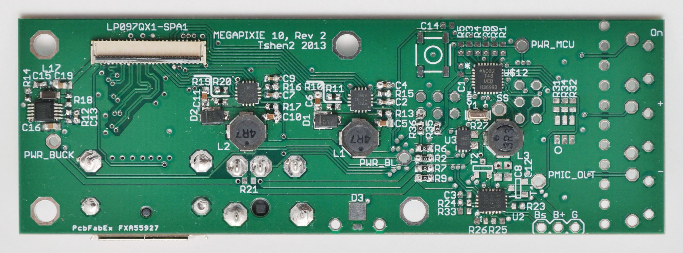
but i was impulsively complicated, so i added a fancy boost-converting backlight driver IC, power-management IC and Li-ion battery into the screen, to keep it running on the go. plus an ATtiny48 to talk to everything through I2C. keeping in mind that two years ago:
- i had zero experience routing differential RF traces, yet was trying to route Displayport signals, which are differential & ultra-ultra-high speed.
- i barely knew how to solder surface-mount components, yet i insisted on using QFN and 0402 packages for everything.
- my PCB skills were in the 'fledgling' stage and this project was hitting way above my weight.
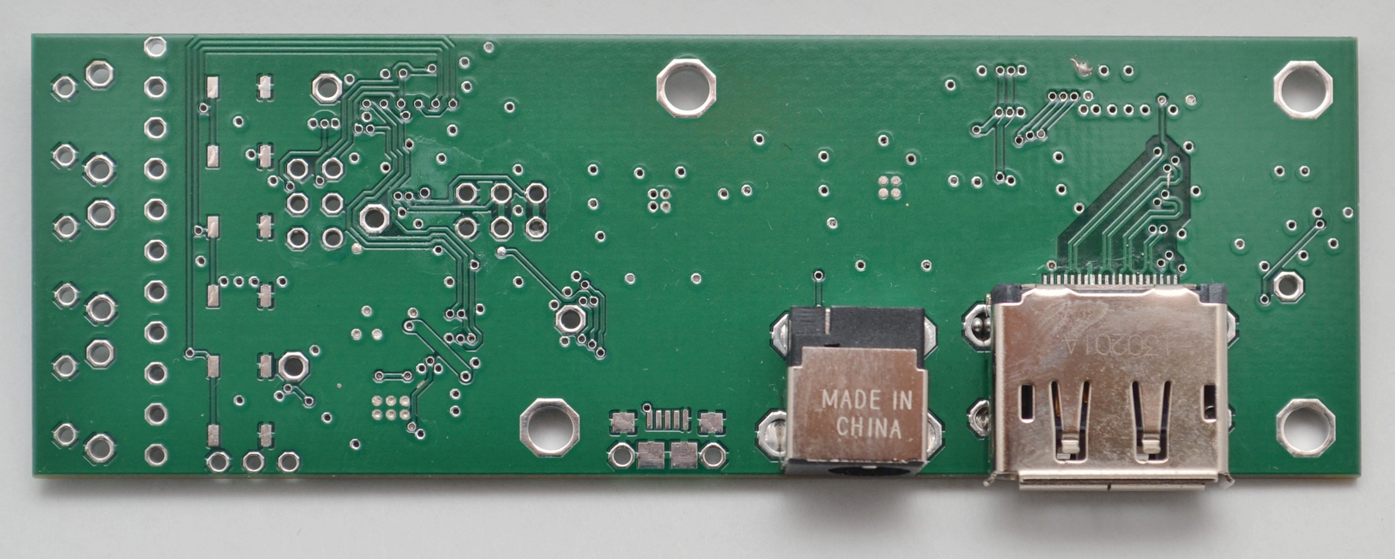
but what the heck, i did it anyway. and here is the result:
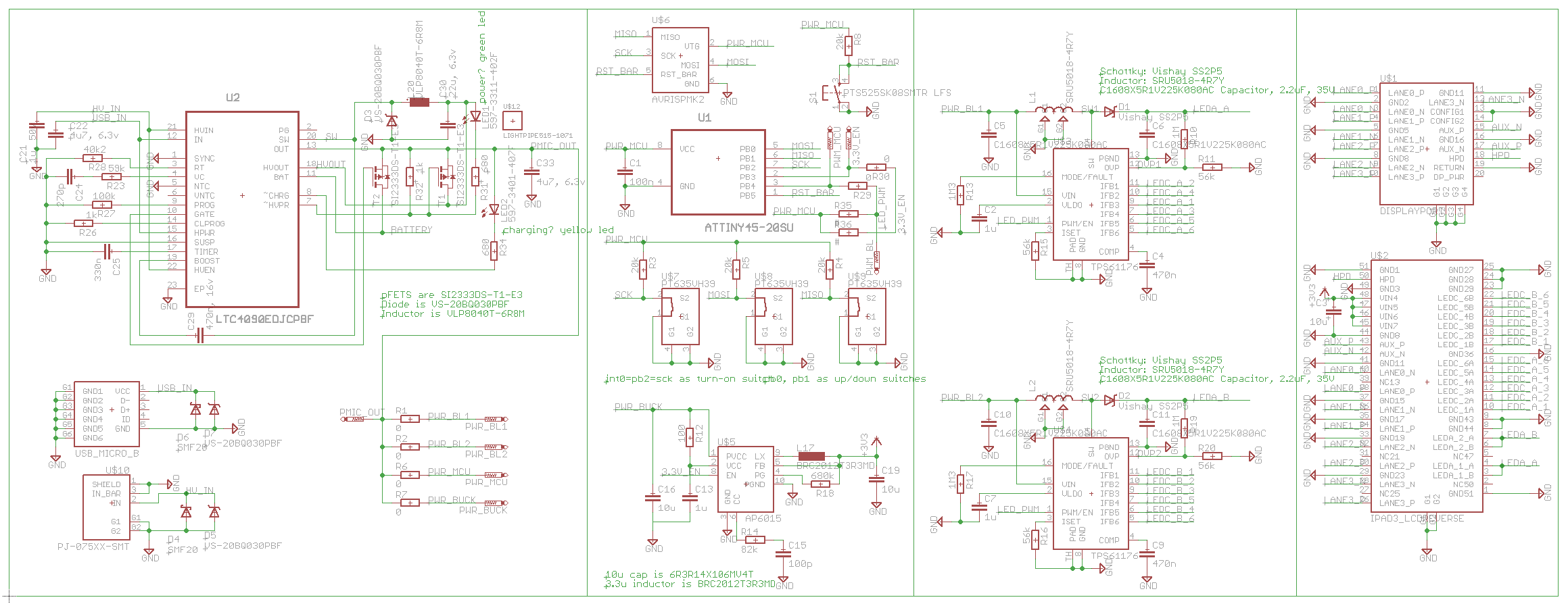
[Retina iPad interface board, attempt #1 - schematic.]
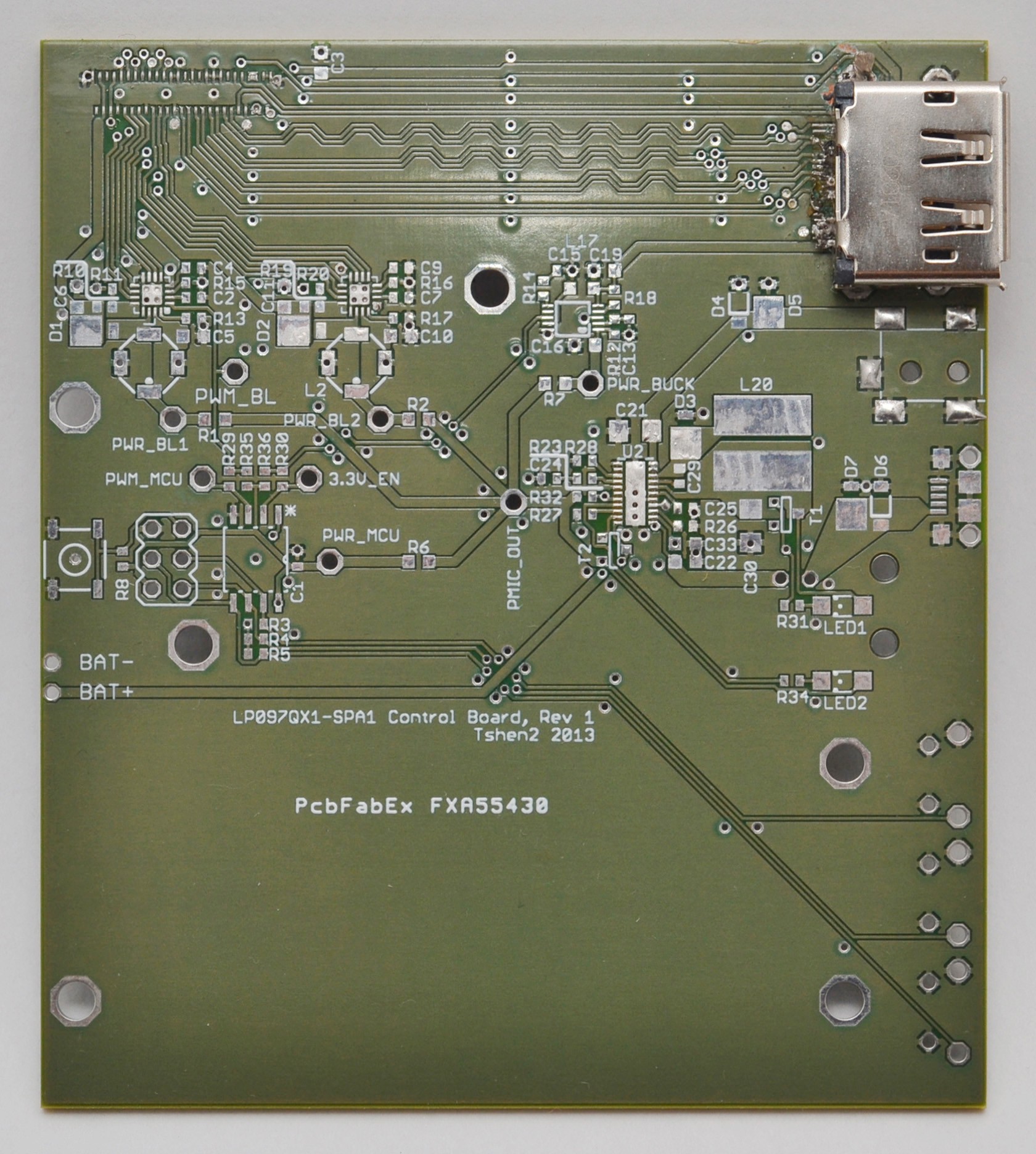
did it work? not at all. it certainly didn't work aesthetically.
i'd also used the Displayport source pinout instead of the sink pinout, which doomed my board from the start. i hadn't even realized there were different source & sink pinouts. i should have dumbed things down, and got the basics right.
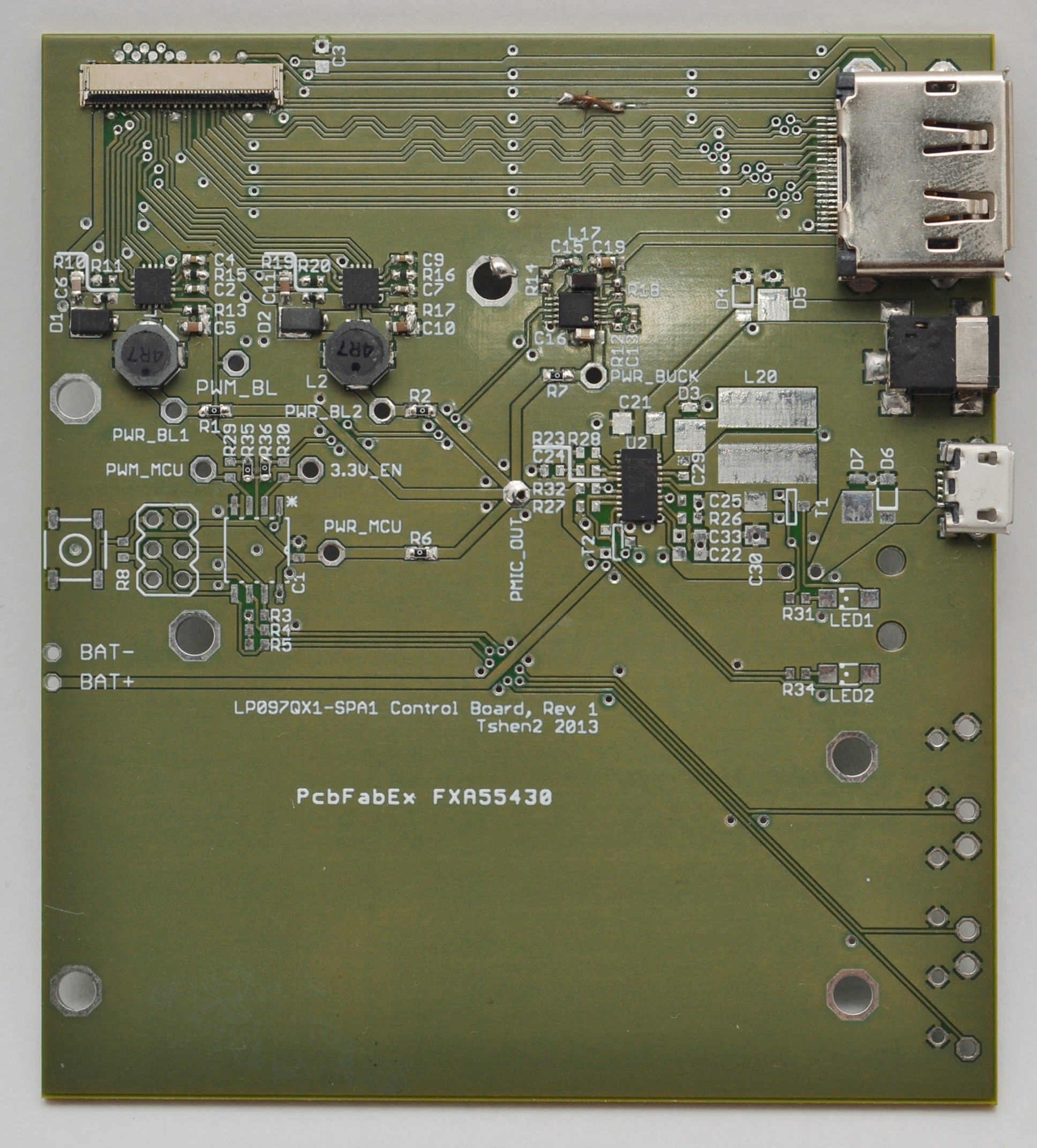
instead i designed another ugly and overly-complicated board because i was clueless in 2013.
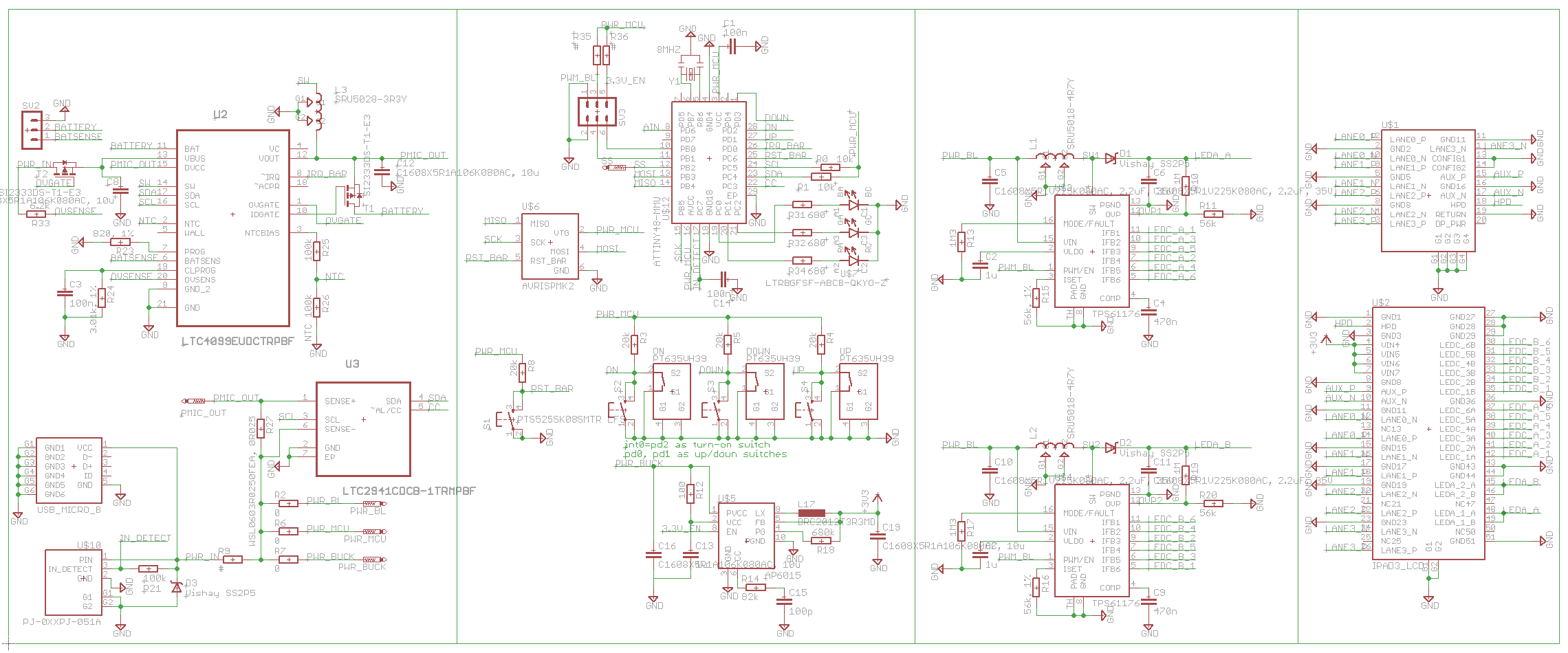
[Retina iPad interface board, attempt #2 - schematic.]
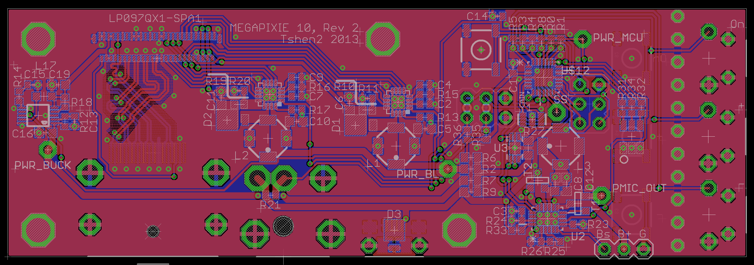
did this work? not even a tiny bit. i still had no idea how to route those high-speed Displayport traces.
this was pretty frustrating. each round of PCB-fabbing cost me a bunch of money. i was buying lots of tiny parts and painstakingly soldering them. nothing was working and i had no clue what i was doing. then i found OSHpark.
OSHpark is a PCB ordering service where the price scales linearly with PCB surface area, with no penalties for number of unique designs. this is unlike my previous PCB source, where i would pay (a lot) for every unique design. this forced me to (rarely) fab-out a very small number of very-complete designs. it didn't encourage experimentation
through OSHpark i could fab PCBs recklessly, ordering a Frankensteinian collection of cheap, small & subtly different boards until i figured out which designs actually worked. i could speed up my development through 'shotgun engineering', trying every possible thing until i pinged upon something which worked.
so in one afternoon, i designed many utterly crude new boards. no more power management, no more fancy backlight, certainly no battery. just a few resistors and two video connectors, connected by those crucial and mysterious high-speed traces. each board had a slight variation of those traces. something, i figured, just had to work.
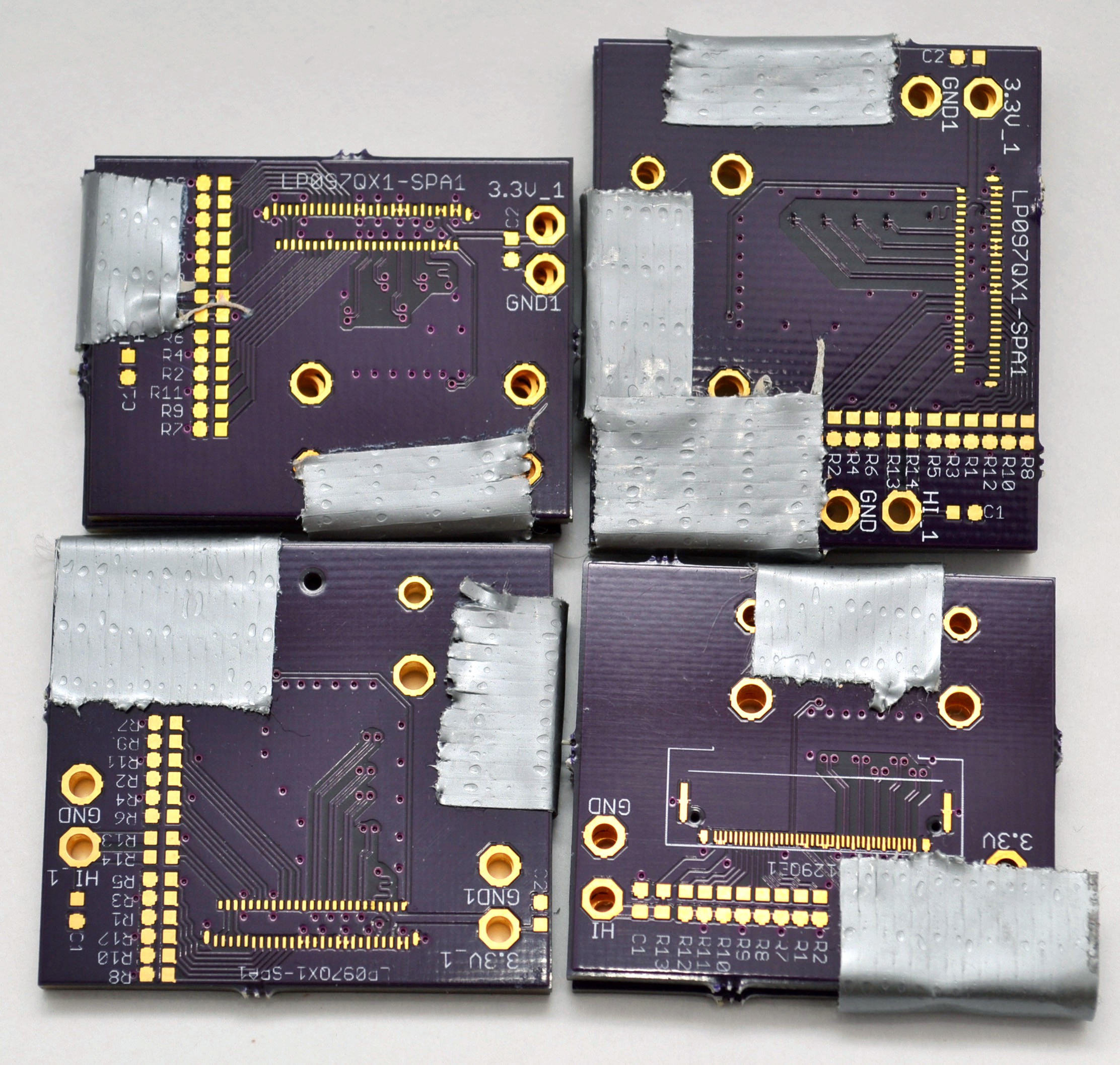
[shotgun engineering.]
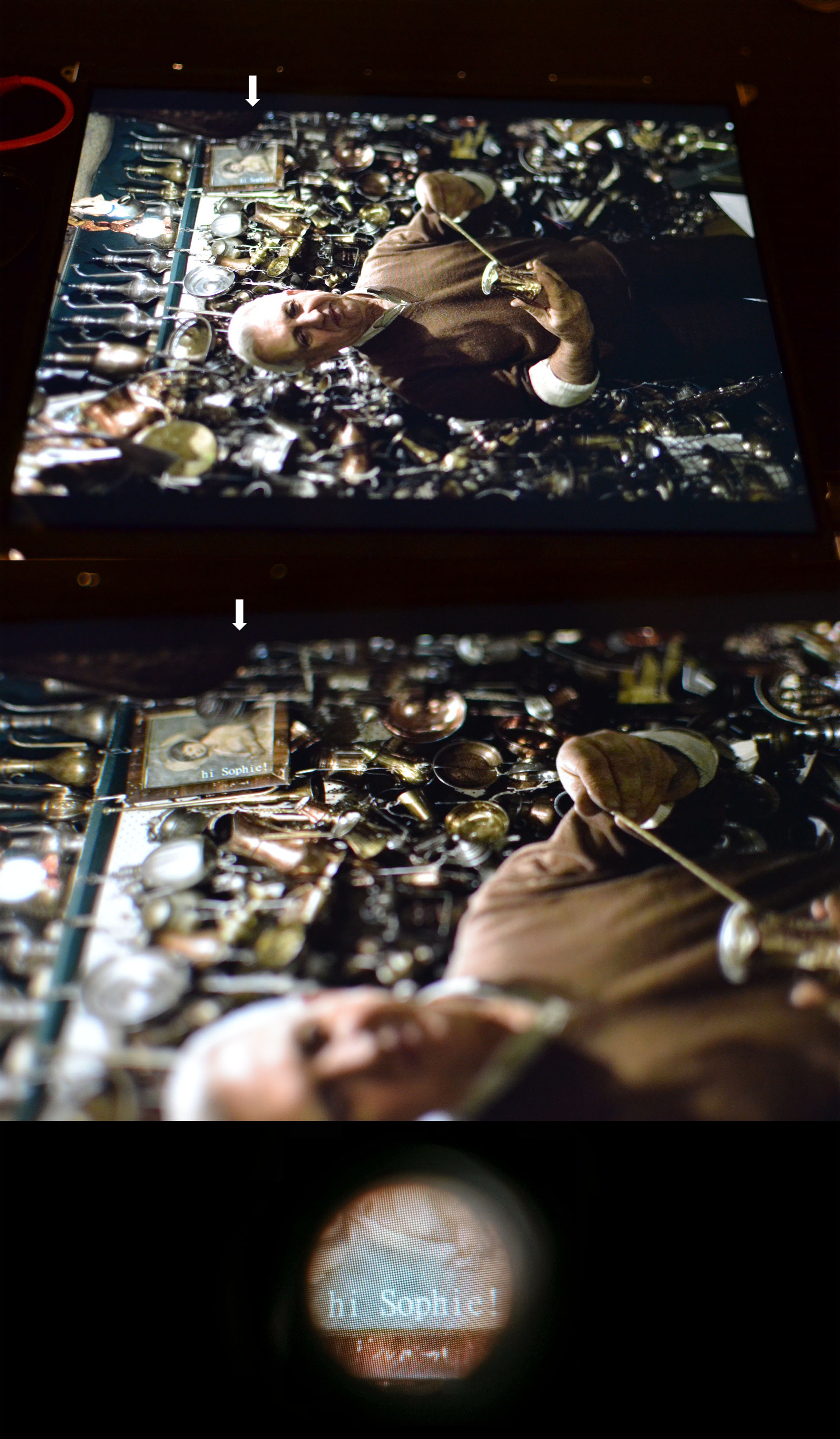
and one did work!
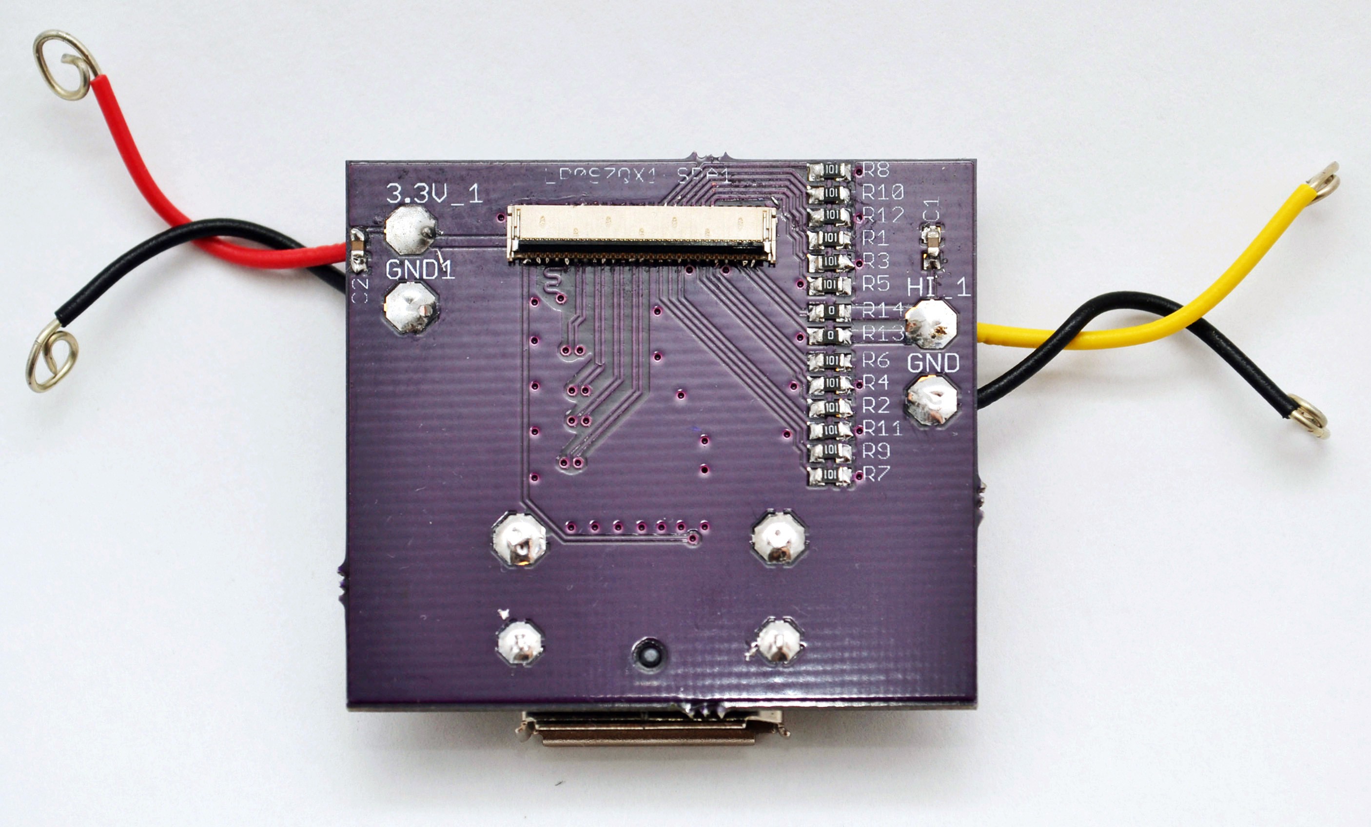
[a winner!]
what should i do with my new Retina screen with super-tiny pixels?
send strange photos to my friend. obviously.
it would be nice to call this a success, but i still didn't trust those high-speed traces. so i decided to test their robustness, by amassing a Displayport cable collection of various lengths.
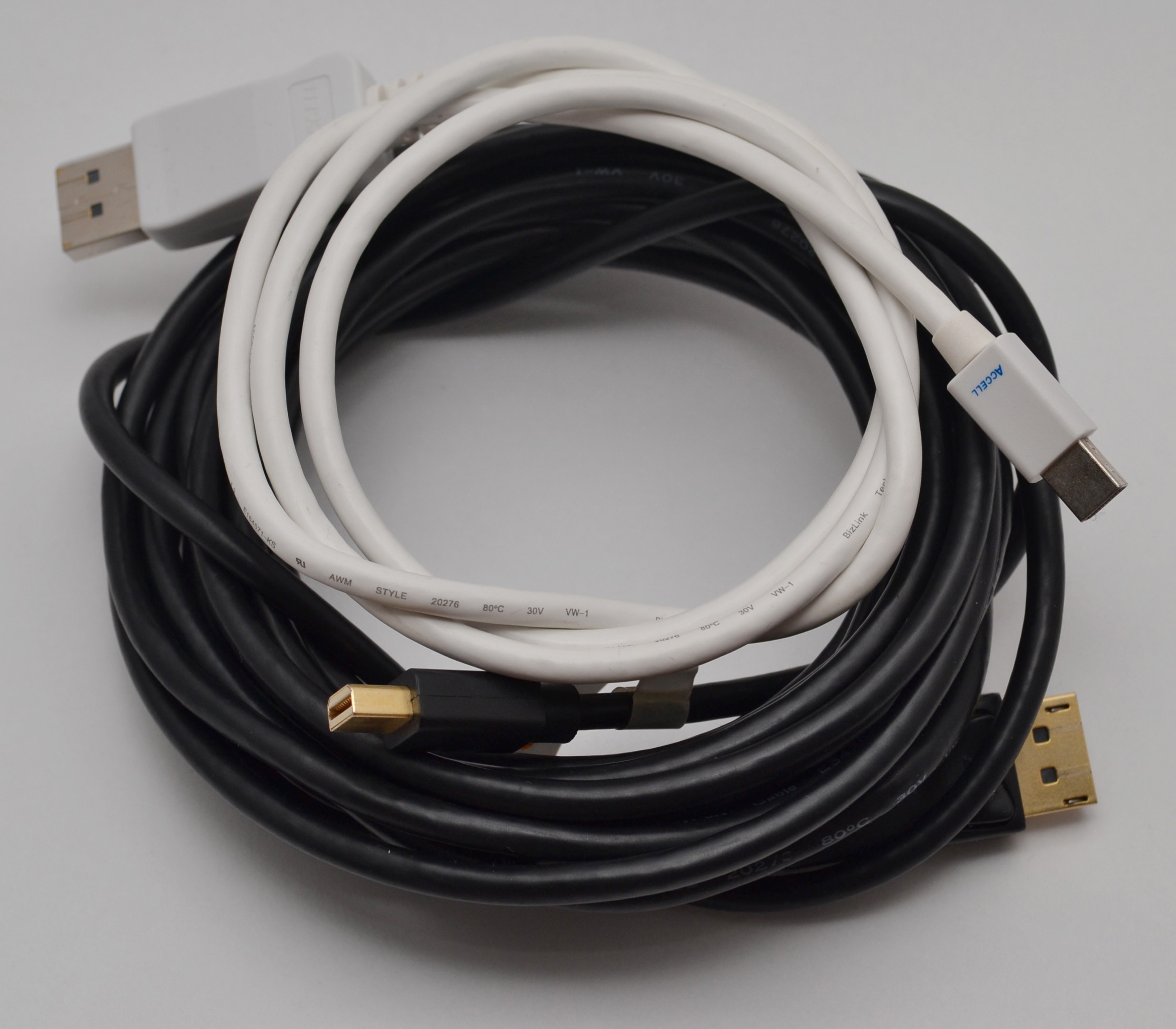
how sensitive was the screen to Displayport signal quality? i had been testing the screen with a 3-foot long Displayport cable, which was hardly strenuous. would it continue working with a 6-foot cable? a 12-foot cable? a 20-foot cable?
alas, anything longer than a 3-foot cable left a garbled mess on the screen. i think it's much harder to get it working over longer distances, which might be why Adafruit previewed this.
at any rate, even the best 9.7" screen is quite useless on a full-sized computer. it was time to move on.
next time: goodbye iPad; tiny cables adventures.
Tshen2 2013
Discussions
Become a Hackaday.io Member
Create an account to leave a comment. Already have an account? Log In.