 Frank Vigilante
Because The Smart Garden is being built as a platform for future robotic gardening systems, I am going to throw cost minimization out the window for the first PCB. It will include many components that serve a redundant purpose. From this platform, I will then be able to reduce the PCB down to a more efficient design. So where do I even begin? In order to answer this question, I decided to gather a good portion of the electronics, and begin to map out my plan for the first board.
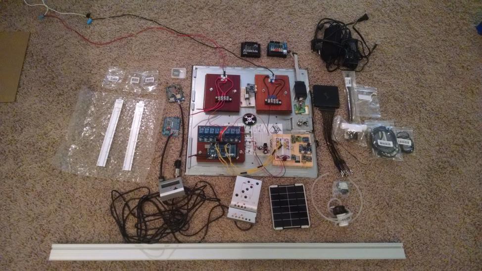
This log will discuss which components shown above will be incorporated into the first PCB, and why....
1. Power supply - The first PCB will take in 12V. It will likely have both, a barrel jack. and terminals so I can alternate between power adapters and solar panel supply (notice the solar charge controller and 12V adapters in the picture).
2. Power Regulation - The PCB will regulate down to 5V and 3.3V. In the picture, you can see a 7805 creating a 5V supply in the breadboard in the middle bottom of the motherboard. The broadboard in the middle top has a 3.3V regulator (but i previously harvested the capacitors). For both of these, I will use really nice heat sinks and capacitors.
3. Relays - I am going to keep using relays because I want to preserve the ability to not only shrink the smart garden design, but also scale it up big! The first PCB will probably have a bank of 14-16 relays.
4. Micro-controller - I see no reason not to put a ATmega2560 in the first PCB. It should be able to handle everything that I want to do.
5. Communication - This is where I am going to get really redundant with the first PCB. In the picture you can see a CC3000, a HC-04 BT module, a ESP8266-12x2, and a RF transmitter/receiver. The first PCB will likely include a CC3000, a ESP8266, and a Nordic semi conductor BT chip, but I am still all over the place on this one. Finally, you can see in the top right of the picture that I have a great wifi antenna ready to be deployed in the garden.
Other Considerations:
- The picture shows some maker slide, and some conductive rubber cord (https://www.adafruit.com/products/519).....this is a hint at my plans for the CNC plant support system.
- A current sensing module is shown in the picture. The represents the inclusion of a component into the PCB that will measure and log energy usage.
- An SD card is shown. This is to back up and preserve all data logged while testing various wireless communication modules.
- I threw some photo resistors and a PIR motion sensor into the picture. The represents how the PCB will have auxiliary ports for adding and removing new sensors.
- I threw my DSlogic (http://store.hackaday.com/products/dslogic) into the picture. This represents all the testing that will need to be done!
Discussions
Become a Hackaday.io Member
Create an account to leave a comment. Already have an account? Log In.