Close
0%
0%

Digital Bench Power Supply

A new design, made from scratch, for a digital bench power supply to offer regulated voltage and current, and prompt shortcircuit protection

Similar projects worth following
As a follow up to one of my earlier regulated power supplies, initially designed to deliver 0..30Volts at up to 10Amps, I have decided it was time for an upgrade. I kept the enclosure and the nice 250W toroidal transformer, and am reshaping everything as a new digital power supply with regulated voltage and current, short circuit protection, lcd display, buzzer for various alarms, temperature sensor on the heat sink and automated protection. Optional bluetooth (HC-05 module) connectivity has been added to the PCB, to allow programming the supply or reading its parameters. For the core of this design I've chosen the well known ATMega8 microcontroller. See http://www.pocketmagic.net/digital-bench-power-supply/

The plan is to design and build a digital bench power supply. As the starting point we have the following:

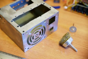
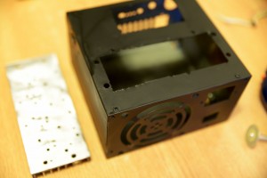
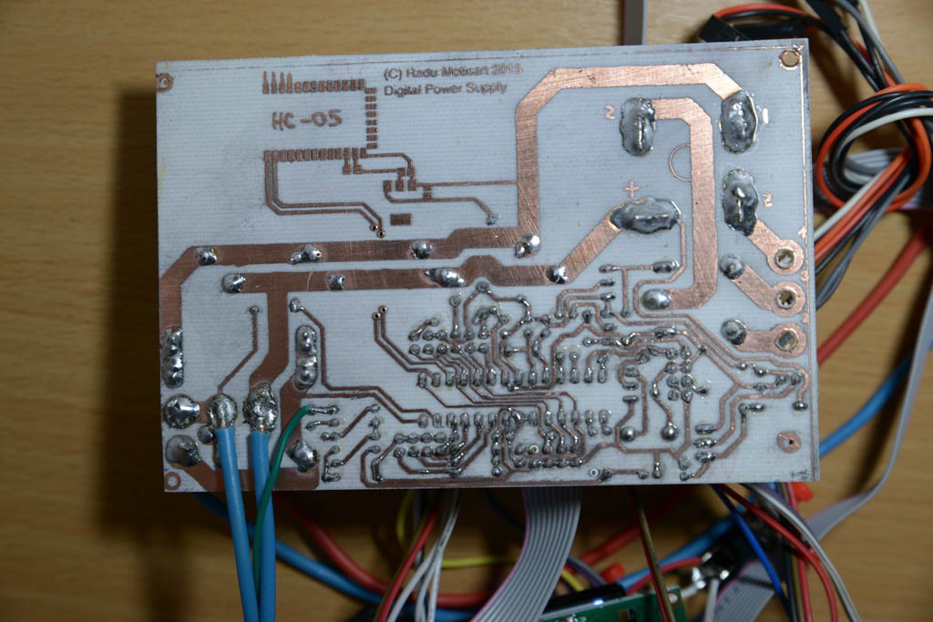
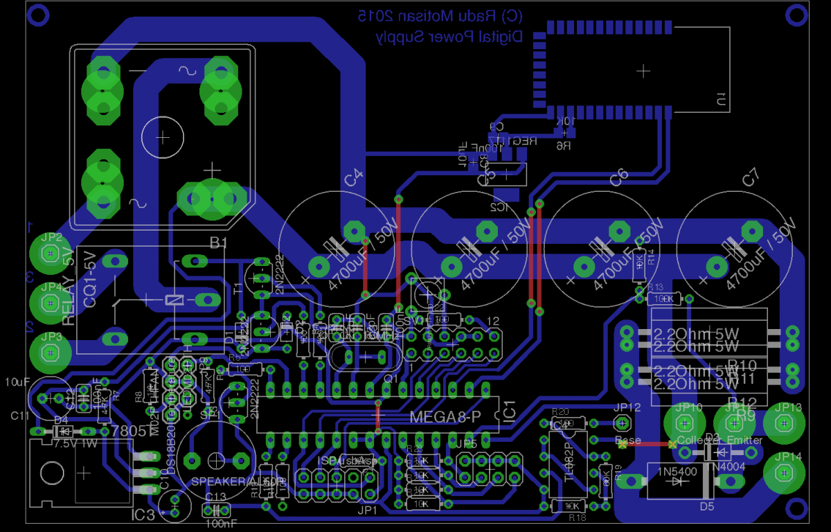
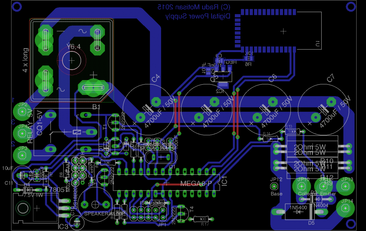
  • a project metallic enclosure from an old ATX supply
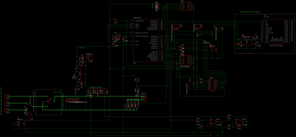
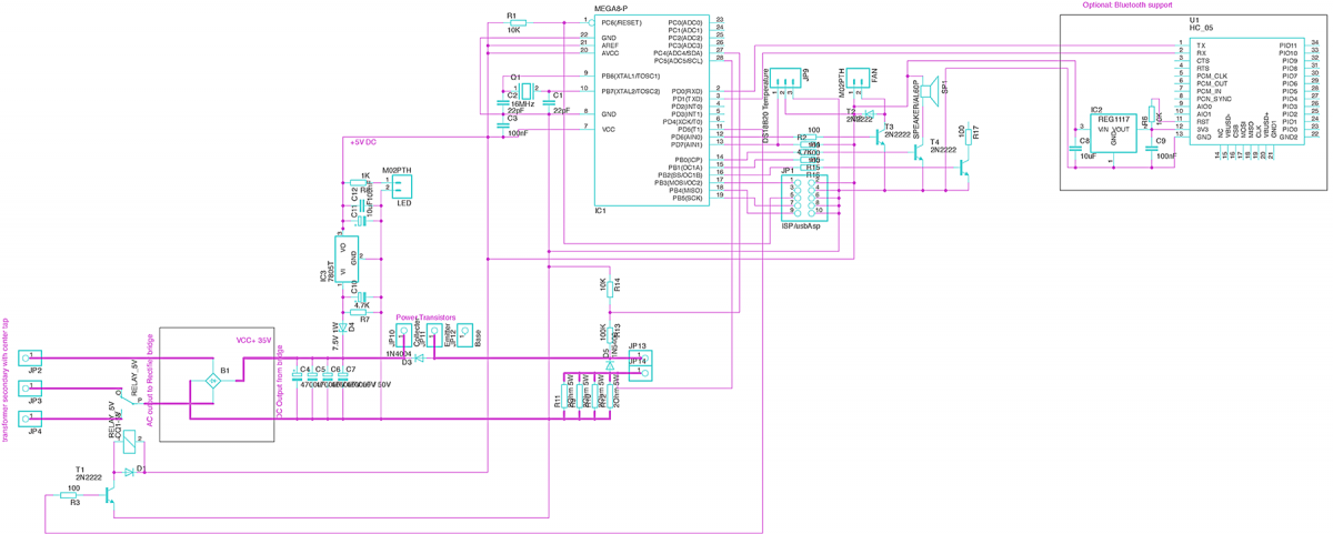
  • a microcontroller, the choice is Atmega8 (or for extended functionality, such as Bluetooth/HC-05, we'd use the Atmega168). This will be the central processing unit for the entire device.
  • a lcd , to display all parameters, most likely a HD44780, either a 2x16 or a 4x20 one.
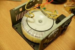
  • a 250W transformer, and a 24VAC secondary with a center tap at 12VAC. Maximum current is 10amps.
  • 4 buttons, to set voltage up/down and current up/down
  • a little self oscillating buzzer to sound the alarm when needed (eg. shortcircuit).

Milestones to implement:

  • the microcontroller is to simplify all hardware design, moving the complexity in the software. This includes driving the LCD, reading the input buttons, measuring the output voltage through a resistive voltage divider connected to an ADC port. Use the measured voltage to display it on screen, but also for the output control block.
  • to support a maximum voltage of 24x1.414 ~= 34Volts, let's make that a round number 35V.
  • output provided through low resistance high power shunt resistors (several connected in parallel to meet the requirements). Using the voltage drop on these resistors, we can calculate the current flowing through them which will be the current output. We use this value for the output control block, to display the current consumption on screen , and for short circuit protection. Critical states or shortcircuit are to be signalled via the buzzer as well.
  • when selected output voltage is 12V or bigger, we use a relay automatically to switch from the center tap to full secondary. And the vice-versa, in order to optimise the power dissipated on the transistors.
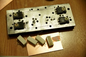
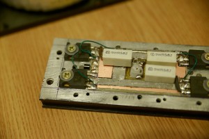
  • output controlled with 4xTIP3055 power transistors connected in parallel on a heatsink with equalising resistors on the emitters.
  • temperature sensor DS18B20 connected on the heatsink to start a fan automatically and with further increasing heating to reduce power to prevent supply damage. Temperature critical events will trigger the buzzer alarm as well.
  • power transistors are to be controlled via a DAC module built either with a R-2R network or a PWM+low pass filter and an amplifier.
digital_power_supply_1-300x200.jpgdigital_power_supply_2-300x200.jpgdigital_power_supply_3-300x200.jpg

Here are the power transistors mounted on the heatsink:

digital_power_supply_4-300x200.jpgdigital_power_supply_5-300x200.jpg

Things to decide / solve:

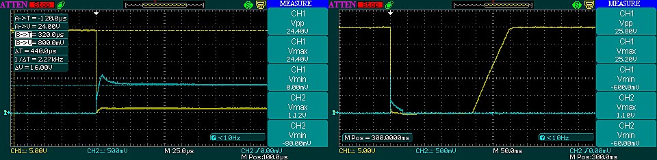
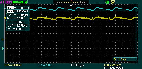
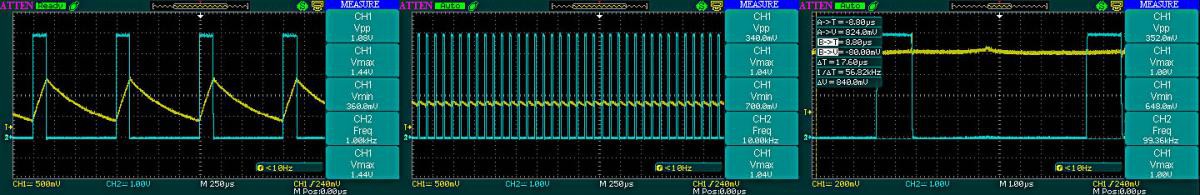
  • the type of DAC to use: either the R/2R or the PWM+Low pass filter. I already did some tests with a Serial Digital to analog converter, presented here.
  • choose the type of display to use, making sure it also fits the case
  • choose a voltage amplifier , needed to boost the DAC output from 0..5V to 0..30V needed to command the base of the power transistors. I can either build one using transistors, either use an Op-amp.
  • I could use an LM358, half with the DAC Low pass filter, and half as an amplifier

That's it for now , feel free to comment or post suggestions.

Edit: the supply has been completed, it works perfectly, and the source code is available on my blog: http://www.pocketmagic.net/digital-bench-power-supply/ . Checkout the log entries for an exciting story from design to completion.

Here is a presentation video to iterate some the functions: https://youtu.be/LduksHuTuo4

  • 1 × Atmega8 Microprocessors, Microcontrollers, DSPs / ARM, RISC-Based Microcontrollers
  • 1 × HD44780 Microprocessors, Microcontrollers, DSPs / Display, Graphics Microcontrollers
  • 4 × Push buttons
  • 1 × TL082 Amplifier and Linear ICs / Operational Amplifiers
  • 1 × Rectifier Bridge

View all 8 components

  • April 18, 2015 - The shortcircuit test

    Radu Motisan04/27/2015 at 14:46 0 comments

    So I tested it for the shortcircuit response time, and the result is that...

    The response is ultra-fast!

    Here are some nice oscillographs showing the quick recovery after a shortcircuit event. It takes less than 350ms to recover to the original voltage configured as shown in the second picture. The CH1 (Yellow) is connected to the output, and the CH2 (Cyan) is connected to the shunt. The first picture shows the quick voltage drop on output, and an increase on the shunt, as expected.
    shortcircuit_response

    A few more tests shown that I can get 26V and 5Amps max with a TL082 and 31.5V and 4Amps max with the LM384, yet the latter is too close to its voltage limits.

    All's done, I'll just update the project description with code and PCB details as well as pictures with my construction. Those of you interested in building one, feel free to ask any questions or send suggestions. Thanks for your interest!

  • April 17, 2015 - first tests

    Radu Motisan04/27/2015 at 14:38 0 comments

    ADC on port PC4 is used to read output voltage through a 10K/100K resistive divider. PC5 is connected to the shunt and used to read the current.

    I measured the transformer output, immediately after the filter capacitors following the rectifier. I get 16.1V with the center tap and 33.8V on the full secondary. With full output, using the TL082, I only get 14.56V vs 16.1V and 26.26V vs 33.8V.

    Finally the PWM code is in place, and I can now adjust not only the duty cycle, to vary the DAC output from 0 to 5V, but also the frequency. I wanted to see the ripple. So I connected the oscilloscope , CH1 (yellow) on the RC low pass filter capacitor and CH2(cyan) on the OpAmp output, right where the signal goes to the base of the power transistors.

    It's not much. The question is what's the best frequency to use with this setup? With a small RC filter cap, it's clear that we need higher frequency values. After a few tests, I opted for 100KHz.

    At 100KHz I get some ripple close to 0.05V, which is good. Next thing to do is to have the output control code in place. As said previously, that needs to be fast. All ADC conversions must be done as interrupts, to avoid the main program loop delaying the critical response (as in case of shortcircuit).

    The only problem is ADC can do a single conversion at a time, so we need to measure voltage and current alternatively since we use two separate ADC channels for that. A 16Mhz crystal is used with the Atmega8 and an ADC prescaler of 128 to increase the conversion speed to maximum. Here's the code logic:

    1) Initialization

    float vref = 5.0;
    
    #define MODE_MEASURE_CURRENT 0
    #define MODE_MEASURE_VOLTAGE 1
    volatile bool adc_mode = MODE_MEASURE_CURRENT;
    volatile float current = 0, voltage = 0; 

    // setup ADC to measure as interrupt: go for current first
    adc_mode = MODE_MEASURE_CURRENT;
    ADMUX = PC5;
    ADCSRA = (1<<ADEN) | (1<<ADIE) | (1<<ADIF) | (1<<ADSC) |
    	(1<<ADPS2) | (1<<ADPS1) | (1<<ADPS0); // set prescaler to 128 (16M/128=125kHz, above 200KHz 10bit results are not reliable)
    sei(); 

    2) interrupt

    // Interrupt service routine for the ADC completion
    // we measure the current (PC5) and the voltage (PC4) alternatively
    ISR(ADC_vect){
      uint16_t analogVal = ADCL | (ADCH << 8);
      if (adc_mode == MODE_MEASURE_CURRENT) {
    	  current = (analogVal / 1024.0 * vref) / 0.55;
    	  // alternate mode
    	  adc_mode = MODE_MEASURE_VOLTAGE;
    	  ADMUX = PC4; // next time we will do ADC on PC4, to get the voltage
      } else if (adc_mode == MODE_MEASURE_VOLTAGE) {
    	  float R14 = 10, //10k
    			R13 = 100; //100K
    	  voltage = analogVal / 1024.0 * (R13 + R14) / R14 * vref;
    	  // alternate mode
    	  adc_mode = MODE_MEASURE_CURRENT;
    	  ADMUX = PC5; // next time we will do ADC on PC5, to get the current
      }
      // Not needed because free-running mode is enabled, so the convertion will restart by itself
      // start another ADC convertion
      //aux_ADCReadIntr(PC5);
      // ADCSRA |= 1<<ADSC;
      ADCSRA = (1<<ADEN) | (1<<ADIE) | (1<<ADIF) /* | (1<<ADFR) */ | (1<<ADSC) |
      				(1<<ADPS2) | (1<<ADPS1) | (1<<ADPS0); // set prescaler to 128 (16M/128=125kHz, above 200KHz 10bit results are not reliable)
    
     }
    Next thing to do is to test the supply for a shortcircuit! In the interrupt code, right in the if (adc_mode == MODE_MEASURE_CURRENT) { , if the current is dangerously high I need to reduce the DAC by lowering the duty cycle, to limit the output. How fast can this be done, is something we need to see.

    fingers crossed...

  • April 16, 2015 - the first PCB prototype is ready

    Radu Motisan04/27/2015 at 13:53 0 comments

    I was able to make a first PCB and write some of the code. The display now works and I can do the first tests. I decided to go with the PWM based DAC. The RC filter output is buffered with the first half of a TL082. The second half is used as a non-inverting amplifier and directly commands the bases of the 4 TIP3055 mounted in parallel on the heatsink. The transistors use equalising resistors of 0.1Ohm / 5W on each emitter.

    I went with the TL082 because of its voltage ratings. Instead of a bipolar source, the plan is to have it hooked on ground and max voltage. It should work fine like that, because all I need is positive output .

    So, this will be an experiment: will it work or will it fry. I just broke my printer's cartridge, and with the last print I was able to do this PCB.

    I surely hope the shortcircuit answer will be fast enough. As for the laser printer cartridges, just a piece of advise for others: don't try cleaning the cylinders!

    The electrolytics should be 50V, but I only had 35V in my toolbox. They're ok for the first tests. Here's the circuit so far:

  • April 8, 2015 - first steps with the design

    Radu Motisan04/27/2015 at 13:30 0 comments

    I started designing the PCB. Here's what I have so far:

    I plan to go with the DAC based on PWM + RC Low pass filter, yet I am concerned about the shortcircuit time of response. If it's not fast enough, the entire work is in vain.

    For the output control block, controlling both the output current and the voltage, will rely on the DAC resolution, but also on the ADC resolution of the feedback loop.

    If ADC is 10bits (max on atmega8), then this will allow us to select voltage levels with in Vo0 = 35x1/2^10 ~= 35mV minimum steps. For 8bits, that's even worse, only 35/2^8~=136mV.

    To help the response time, a solution is to do all time critical operations as interrupts, for example the ADC convertions responsabile for reading voltage and current.

View all 4 project logs

  • 1
    Step 1

    You'll need a transformer and a suitable box / enclosure. Find these first.

  • 2
    Step 2

    Find a heatsink for the transistors. Mount them there, including the emitter current equalising resistors. Mount the entire assembly on your project's enclosure

  • 3
    Step 3

    Build the PCB using your preferred method. I designed this with through hole components, so anyone can solder this circuit. Complete your board, connect it to the transformer, LCD, and buttons.

View all 5 instructions

Enjoy this project?

Share

Discussions

Similar Projects

Does this project spark your interest?

Become a member to follow this project and never miss any updates