When I got home from work, a familiar purple envelope was waiting for me. I fired up my microscope and inspected the PCB:s straight away. This is the first time I have ordered 4-layer PCB:s from OSHpark.com, and I was anxious to see how they turned out.
Notice how the copper pour is not centered in the board? The alignment is OK in the left/right direction, and a bit worse in the up/down direction. We can rule out a problem with the Gerber files by looking at how far into the board the "mouse bites" extend. At the top and bottom edges, the drilled hole edges extends past or does not reach the board outline respectively, indicating that the drilling and routing stages could be aligned better. The mouse bites are drilled together with all the other holes (before plating and etching), but the outline is routed as the very last stage in production.
I could not get a good photo of if, but if I look directly at the bottom edge, I can see the stitching vias through the fiberglass. When I sanded the remains of the mouse bite away, the sand paper bit into them, exposing copper.
This small misalignment is not a problem for me, just something I need to remember to take into account for the next revision. I'll check with OSHpark if I should expect better in the future.
![]()
The outer dimensions are 0.1 mm larger than nominal, but that is well within tolerances and the board fits exactly as it is supposed to!
![]() Other than the outline alignment issue, the board is stunningly beautiful! The purple solder mask on this board is less glossy compared to the 2-layer boards I have bought previously, and it looks a bit more refined. The soldermask alignment is perfect, and the silkscreen is easily on par with boards that cost ten times as much! The drill alignment is also very good.
Other than the outline alignment issue, the board is stunningly beautiful! The purple solder mask on this board is less glossy compared to the 2-layer boards I have bought previously, and it looks a bit more refined. The soldermask alignment is perfect, and the silkscreen is easily on par with boards that cost ten times as much! The drill alignment is also very good.
In the image below, the component designators are approx. 0.65 mm high, and the text is still razor sharp and extremely easy to read. Really, really good looking! The breaks at some points are due to collisions with vias, and not a problem with the printing.
If you look at the curve of the copper pour, you can see that it does not follow the board edge evenly. This is also due to the slight misalignment.
![]()
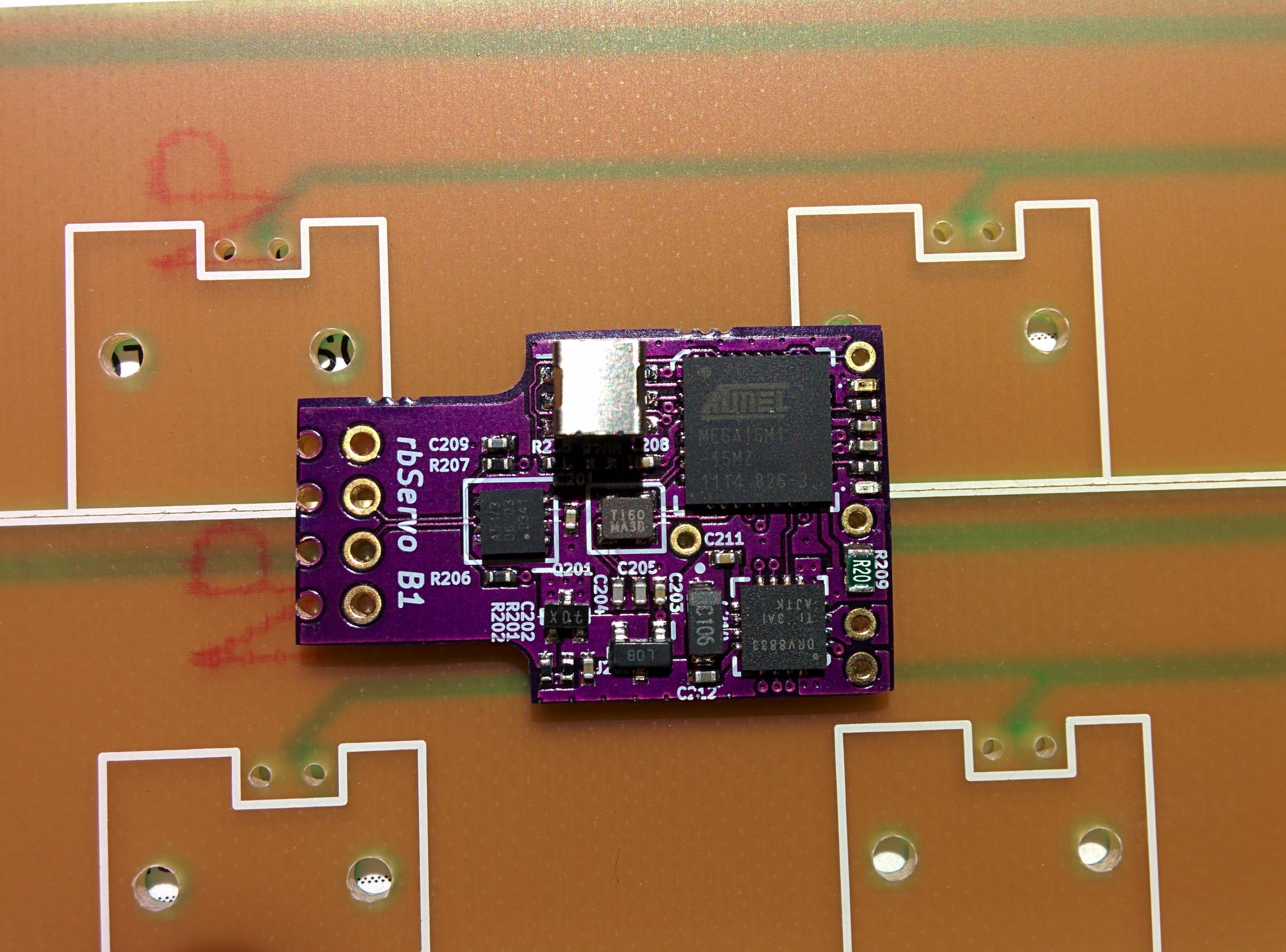
After solder paste printing, component placement and hot air reflow the board came out looking like this:
![]()
![]()
I used a solder stencil from OSHstencils.com this time, and it worked really well. I could not see that it was in any way worse than the stencils I have ordered from ohararp.com, but they were a lot cheaper!
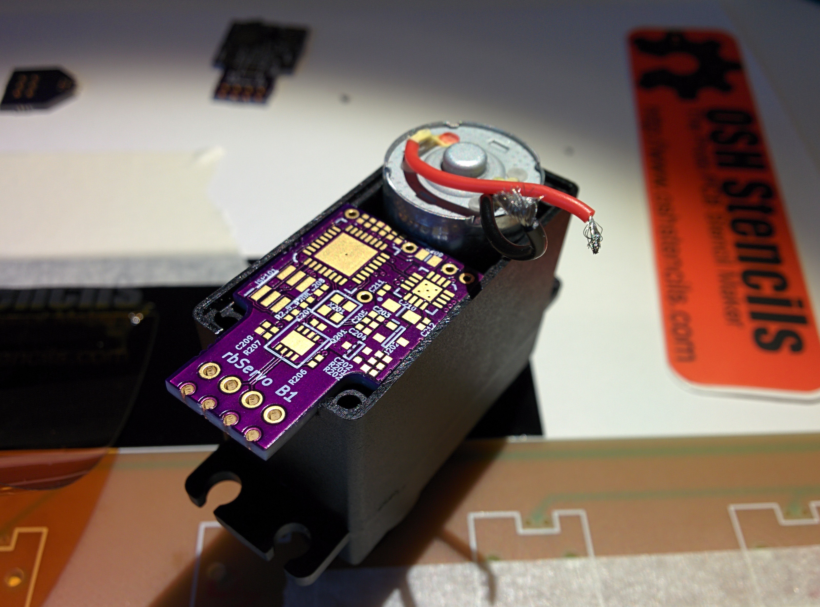
The corners are a bit rounded in this pic, I need to be more careful when sanding the mouse bites away.
The next step is to try them out, but that is for another update.
 RasmusB
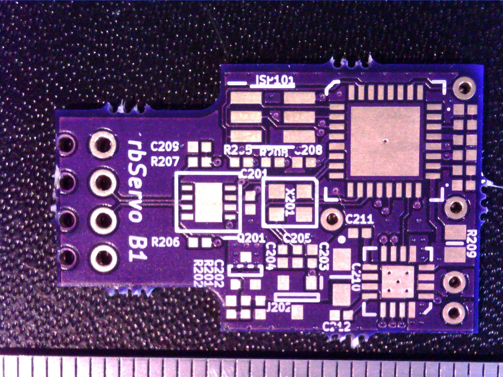
 Other than the outline alignment issue, the board is stunningly beautiful! The purple solder mask on this board is less glossy compared to the 2-layer boards I have bought previously, and it looks a bit more refined. The soldermask alignment is perfect, and the silkscreen is easily on par with boards that cost ten times as much! The drill alignment is also very good.
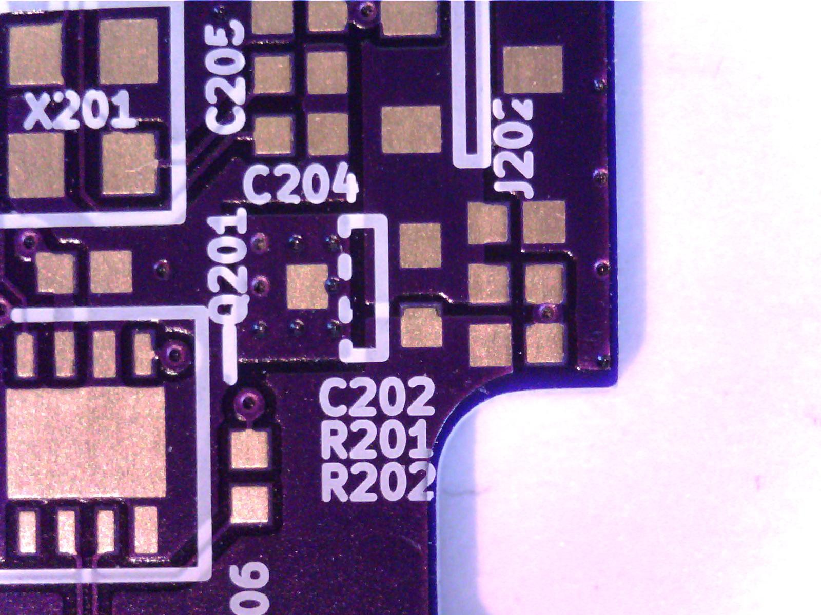
Discussions
Become a Hackaday.io Member
Create an account to leave a comment. Already have an account? Log In.