 Jean-François Duval
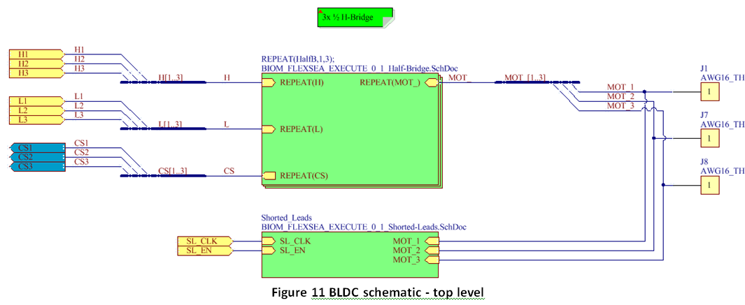
The BLDC schematic consists of 3 copies of the Half-bridge sheet (motor commutation), the Shorted-Leads protection circuit, phase voltage sensing and bridge temperature sensing.
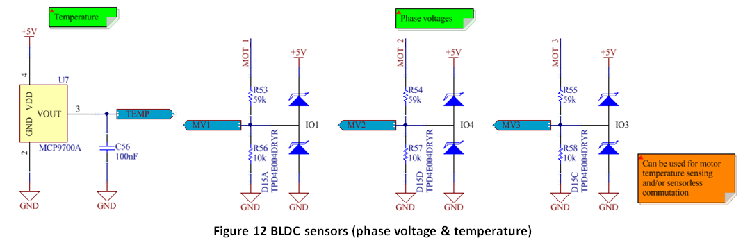
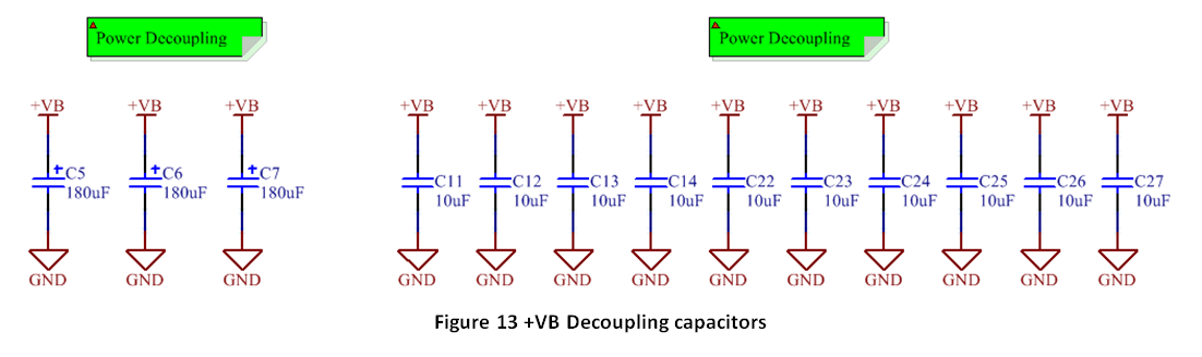
U7 (temperature sensor) is routed close to the power MOSFETs. Figure 13 shows the decoupling capacitors present on the Power Supply schematic sheet. They are mainly used for the BLDC driver. C11-14 & C22-27 are relatively small ceramic capacitors. Their total value, 100µF, is not sufficient to guarantee that the bus voltage won’t exceed the limits if a large amount of regeneration is done. C5 to C7 are used to absorb all this energy (and to provide power during switching transitions as well), but they are bulky. In applications were volume is highly constrained, C5-7 can be removed if an external protection circuit is added to the system (typically, a bus-dump semiconductor or resistor). This should be done with care.
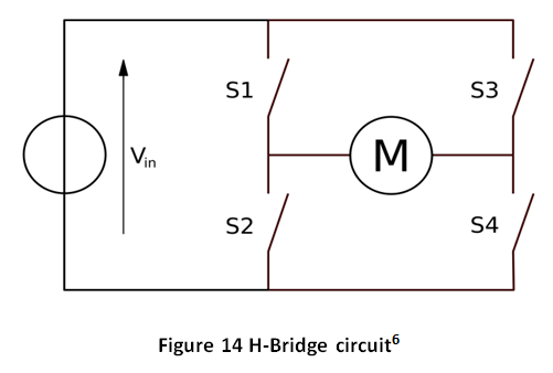 DC motors are commonly driven by a circuit called an H-Bridge. An H bridge is an electronic circuit that enables a voltage to be applied across a load in either direction. Closing S1 and S4 will make the motor turn in one direction, while closing S2 and S3 will make it rotate in the opposite direction. Closing S1 and S3, or S2 and S4, can be used to brake the motor. Closing S1 and S2, or S3 and S4, will create a short circuit on the power supply and can lead to catastrophic failure.
The switches in the above schematic can be relay contacts, bipolar transistors, MOSFETs or IGBTs. MOSFETs offer the best efficiency for low-voltage applications.
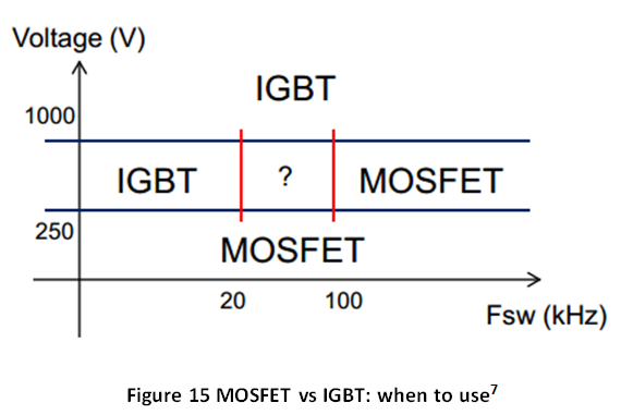
For low-voltage high-frequency application such as ours MOSFETs are the most common solution. A good reason not to use IGBTs is that a distributor like Digikey doesn't carry devices rated for less than 300V, and the smallest SMT package available is DPAK.
“The selection of a P-channel or N-channel load switch depends on the specific needs of the application. The N-channel MOSFET has several advantages over the P-channel MOSFET. For example, the N-channel majority carriers (electrons) have a higher mobility than the P-channel majority carriers (holes). Because of this, the N-channel transistor has lower RDS(on) and gate capacitance for the same die area. Thus, for high current applications the N-channel transistor is preferred.” [8]
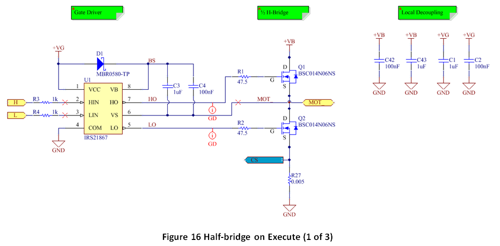
A voltage of 10V from the Gate to the Source (noted VGS) is required to fully turn on an N-Channel MOSFET. The source of the high side switch can swing from the lowest system voltage to the highest. To turn the high-side switch on we need a voltage higher than the motor voltage, typically the highest voltage in a system.
“A gate driver is a power amplifier that accepts a low-power input from a controller IC and produces a high-current drive input for the gate of a high-power transistor such as an IGBT or power MOSFET. Gate drivers can be provided either on-chip or as a discrete module. In essence, a gate driver consists of a level shifter in combination with an amplifier.” [9]
The IRS21867 was selected because of its robustness, especially for its tolerance to negative transient voltages. For the MOSFETs, the QFN 5x6 package (also known as 8-PowerTDFN and PG-TDSON-8) was selected for its small size, its wide industry acceptance and the convenience of doing bottom cooling.
The BSC014N06NS MOSFETs were selected for their availability, price, low RDSON and low gate capacitance. As a safety margin, MOSFETs rated for at least twice the bus voltage (28V Max) were selected. At 60V, the BSC014N06NS are protected in case of really bad inductive spikes.
The R1 and R2 gate resistors were selected from what could be called an “educated arbitrarily decision” as a compromise value between fast switching and slow switching. Switching too slowly can introduce shoot-through and increase switching losses, while switching too fast can increase the transient voltages generated (can lead to more noise, and to component destruction in extreme cases). The efficiency of the motor driver can be augmented by carefully selecting gate resistors and by doing a careful selection of semiconductors, but this optimization is outside of the scope of this work.
R27 is used for current sensing.
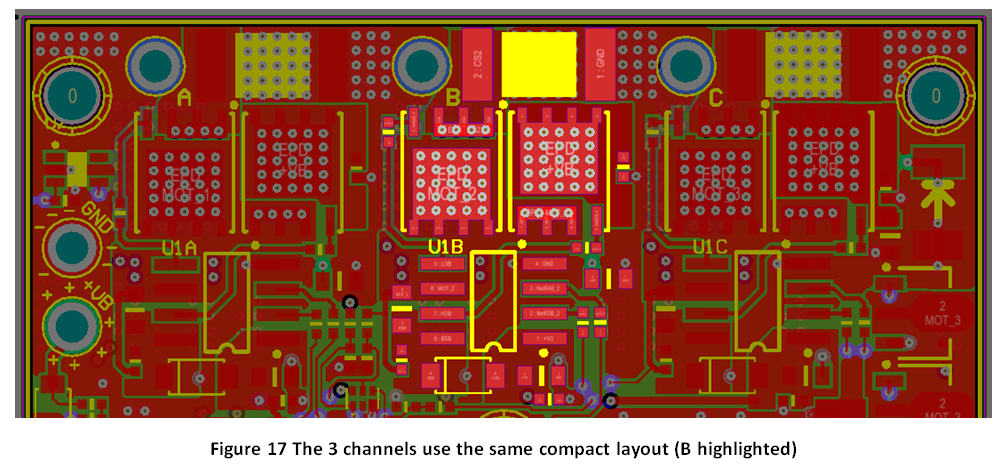
As can be seen on Figure 17 a large number of vias are used. They serve two purposes: thermal transfer and layer “tying”. This PCB has 6 layers:
- Layer 1: Top components, signals and small planes
- Layers 2 and 5: Ground planes
- Layer 3: Power. Top half is a +VB plane, Bottom half is a +5V plane.
- Layer 4: Mixed. In the context of the bridges, it is used for the MOT nets and for +VB.
- Layer 6: Bottom components, interface to the heat sink (so a maximum plane area is used around the bridges).
The critical power paths are always shared by a minimum of two layers.
[6] http://en.wikipedia.org/wiki/H_bridge
Discussions
Become a Hackaday.io Member
Create an account to leave a comment. Already have an account? Log In.