Wenting Zhang
-
3 year recap and future plans
02/28/2021 at 20:09 • 0 commentsHi everyone. It's now end of February of 2021 as I am writing this. The VerilogBoy project was started back in February of 2018, and it has been 3 years since I have started this. I would just like to recap what have been achieved and the future plans of this project.
What has been done
Original Prototype on ML505
I started this project as a course project for the CMPEN275 (Digital Design Lab) back in Penn State. I implemented the whole thing on the ML505 FPGA dev board. By the end of the term I was able to get Pokemon running on the board as a demo. I wrote my own PSG, PPU, and timer, but reused the CPU from one of the open source FPGA GB project.
Unfortunately no recording of the presentation was available, otherwise personally I would really love to watch that again... The only thing I have from that time was a recording showing it running (captured via VGA, didn't capture sound):
Improving the Code
The original code works, but not great. It fails lot of the test ROMs available. After learning the internal architectures of the GB CPU (SM83), I rewrote the CPU myself, two times. It should be now cycle accurate.
To help test everything, I have also created a Verilated simulator that runs on PC. It could loads the ROM and runs the code in the simulated VerilogBoy. On Apple M1 Macs, it could runs up to close to real time speed (4MHz). As a reference, I used isim bundled with Xilinx ISE to simulate the design back in 2018 to aid debugging. It runs at around 2kHz.
Building a handheld
I have been working on creating an FPGA based handheld device that would work with my VerilogBoy.
I build 2 revisions of the device in total:
Rev 0.0 in September 2018. It was the first revision, with dedicated MCU for controlling the hardware. But I had some serious bugs in the design.
Rev 0.1 in December 2020. I removed the dedicated MCU because I thought I can just use FSMs and reuse the main GB CPU (turns out it was a bad idea) and fixed several bugs. This is the revision I showed people during the VCF and Latch-up conf.
See a demo here: https://twitter.com/zephray_wenting/status/1119956214752907264
After that I was working on designing the rev 0.2, with a dedicated MCU and a dedicated MIPI DSI bridge chip, But I didn't had much time in 2020 to really execute the project. So that stays as an unfinished PCB design.
Porting to the Pano Logic
I have a whole series of project logs about porting this thing to the Pano Logic G1 device, which is a small FPGA thin client:
A detour to the Pano Logic G1 (1) - LPDDR
A detour to the Pano Logic G1 (2) - Cache
A detour to Pano Logic G1 (3) - UART & Hard fault
A detour to Pano Logic G1 (4) - USB
It worked at last, and I am quite happy about that.
Going forward
Possible improvements to the code
The first thing would be the PPU. I never get to refactor the PPU code. It was quite messy. It also fails lot of the cycle accuracy tests.
The second thing would be extend the code to support GBC mode. This could be potentially combined with the first one, because the GBC mostly demands an enhanced PPU.
I do not have plan to do any of these in the near future.
The handheld
Though I didn't had much time to play with the handheld design back in 2020, I am hoping to spend more time on it in 2021. I have renamed the handheld to Fobu to avoid confusion, also denoting as a shift of the focus. Rather than a handheld designed to run VerilogBoy, but it would be a handheld targeting 2 use cases:
1. Handheld FPGA chiptune player
2. FPGA retro gaming in both handheld and docked mode
The project would have its own page: https://hackaday.io/project/177963-fobu
-
A detour to Pano Logic G1 (4) - USB
02/28/2021 at 17:31 • 0 comments![]() I promised that there would be an update about the USB, here it is. This update would only talk about the USB 2.0 Host on the Pano Logic G1 devices with ISP1760 USB host controller, so it is probably not applicable to other platforms. The goal here is to write a set of RTL and software stack, so it is possible to use USB HID joystick/ gamepad and USB mass storage devices on the Pano G1. Speed would not be the concern here.
I promised that there would be an update about the USB, here it is. This update would only talk about the USB 2.0 Host on the Pano Logic G1 devices with ISP1760 USB host controller, so it is probably not applicable to other platforms. The goal here is to write a set of RTL and software stack, so it is possible to use USB HID joystick/ gamepad and USB mass storage devices on the Pano G1. Speed would not be the concern here.Hardware Connections
On the Pano G1, an USB 2.0 high-speed host controller (Phillips ISP1760) is connected to the FPGA via 16-bit parallel memory bus. To mitigate one of the controller’s errata, an USB high speed hub (SMSC USB2513) is connected to one of the downstream port of the controller, and all user accessible ports are connected to the USB hub.
Overall Architecture
Though it might be possible to write a FSM to implement some basics of the USB host protocol stack, it is just not very practical. (Device side might be more practical, though). The solution I have here is to continue use the PicoRV32 soft-core processor on the FPGA. The host controller would be mapped to PicoRV32’s memory space as MMIO, then software driver and protocol stack can run on the PicoRV32. When needed, certain outputs can be achieved by using MMIO GPIO (for example, output the currently pressed keys). Hopefully, debugging software would be much easier than debugging hardware.
Generally, there would be several layers. The bottom part is called as the HCD (Host Controller Driver), which is specific to particular hardware, like the controller chip being used. Then it comes the HD (Host Driver), this is the part handles device enumeration and USB Hub communication, this layer is no longer specific to the platform. Higher than that is the class driver, as name suggests this is specific to a device class, for example, HID class or audio class. The driver might be generic to the whole class, or it might just support one of few specific USB devices. Higher than that, usually it is operating system, or in our case, user application.
In conclusion, there are 5 things I need to do:
- Write the RTL to interface ISP1760 with PicoRV32
- Port or write the HCD for ISP1760
- Port some appropriate host driver over
- Port or write the class driver for HID gamepad and mass storage devices
- Write some application code to use the driver
Let’s discuss all these parts.
MMIO interface
This is the easiest part. It is a pretty standard parallel async MMIO interface. Though there are DMA modes, but I am not going to support them anyway so forget about these. The address space is 64KB, so there should be 16 address lines. As the data bus width is 16 bit, and the access is always half-word aligned, the lowest line is omitted, leaving 15 address lines. However, here it has A[17:1], in total of 17 address lines. According to the datasheet, the upper 2 bits are used to denote the currently accessing page, and the device allows opening multiple pages at the same time… Sounds like that of SDRAM. As I said speed wouldn’t be the concern here, so they are never used in my code. Otherwise it’s fairly standard. Just to make it even simpler, I didn’t to the bitwidth conversion logic, the low 16bits of the data bus is connected to the low 16bits of the CPU, and high 16bits are left unconnected. Thus it is occupying twice the address space as it should, and all addresses should be shifted by one to compensate the wasted bitwidth.
HUBs
Before I talk about the USB protocol stack, I want to talk more about USB hubs. The architecture of Pano G1’s USB is basically, full of hubs. In the hardware, there is one USB Hub chip, but that’s not all.
According to the EHCI (Enhanced Host Controller Interface) specification (the standard USB 2.0 host controller specification), a USB 2.0 high speed host controller would be only able to communicate with high speed devices. No full speed or low speed devices are possible here. To implement an USB host that is compatible to both types of devices, one would need to incorporate an additional OHCI (Open Host Controller Interface) or UHCI (Universal Host Controller Interface) compatible controller into the system, then use an analog switch to switch to them when the connected device is a low-speed or full-speed one.
Well, this sounds, stupid. Why would one need to put two controller chips in the system for one USB port and switch between them? Is it possible to design one controller that is capable handling both type of devices?
Well it is possible, and such controllers do exist. It is called as TDI controller in the Linux kernel, TDI refers the company TransDimension, which developed such kind of controller. The company later was renamed to Oxford semiconductor, acquired by PLX technology, and then acquired by Broadcom. The general idea is using a transaction-translator (TT) from the USB 2.0 specification (but not part of EHCI specification). The user can plug in USB devices with different speeds on the same hub, however to maximize the throughput, the USB hub should always communicate with the upstream using high speed mode. This means the hub must have some way to interface with LS or HS devices and transfer the LS/HS data through a HS port. This is exactly what needed: the ECHI controller could only provide one HS port. TT could adapt a LS or FS device to a HS port. TDI controller is basically a standard EHCI controller with a TT, as well as few additional registers to control the embedded TT.
Or, without modifying the controller, one can just connect a standard USB 2.0 hub to the EHCI controller, and the hub would handle that nicely. This is the way Philips did that: in the ISP1760, there is one integrated Philips ISP1520 USB 2.0 Hub, directly connected to the host controller inside the chip. I am not sure how this connection is done internally, but it doesn’t matter from driver’s perspective, it is just one hub connected to one of the DFP (downstream facing port). Now there is in total of 2 hubs in the device.
But there could be a third one: the root hub. In the device manager of a Windows PC, one can see these root hubs. For example, this is a screenshot of the device manager on my PC:
![1560125591219-usb-devices.png]() What are these? Is there always one embedded hub in the controller? Not really. The host driver sometimes needs to control the port. For example, turn on or off the power supply of a specific port, or reset a specific port. For USB hubs, they are implemented as control packets sent to the USB hub, the hub would receive these packs and function accordingly. But to control ports on an EHCI compatible controller, one would need to use MMIO to modify certain registers to accomplish the same thing. From the driver interface perspective, this is inconvenient: there would be two different interfaces to do the same thing. As a result, generally in the HCD (host controller driver), there would be some code to emulate a hub: it would intercept control packets sent to endpoint 0, reports itself as a USB hub, and write values to MMIO when certain control packets are being received. So there would be a third hub in the system. Imagine our poor packet would have to go through at least three hubs before it can reach the other end… And our protocol stack must be able to handle multiple layers of hub as well.
What are these? Is there always one embedded hub in the controller? Not really. The host driver sometimes needs to control the port. For example, turn on or off the power supply of a specific port, or reset a specific port. For USB hubs, they are implemented as control packets sent to the USB hub, the hub would receive these packs and function accordingly. But to control ports on an EHCI compatible controller, one would need to use MMIO to modify certain registers to accomplish the same thing. From the driver interface perspective, this is inconvenient: there would be two different interfaces to do the same thing. As a result, generally in the HCD (host controller driver), there would be some code to emulate a hub: it would intercept control packets sent to endpoint 0, reports itself as a USB hub, and write values to MMIO when certain control packets are being received. So there would be a third hub in the system. Imagine our poor packet would have to go through at least three hubs before it can reach the other end… And our protocol stack must be able to handle multiple layers of hub as well.Though luckily, on ISP1760, the third layer is optional: the ISP1760 HC (host controller) only has one DFP, and it is always connected to the integrated ISP1520 hub. There is generally no reason for the software to control this DFP after it is running, so we might just hardcode these register configurations. Then the integrated ISP1520 would become the root hub. But then the system still has 2 hubs to go through.
Host Driver
The next step would be HCD. But as the HCD highly depends on the host driver, I need to decide which host driver to use first. Generally, this is about picking a USB host stack to use. I really don’t want to waste my time reinventing another wheel here, not talking about the difficulties of debugging many things at the same time.
The first one I found is called the TinyUSB. Unfortunately, as its README points out, it does not support cascading hubs. I assume this is something limited by their architecture, and probably not something that can be easily supported without refactoring a lot of code. But their code is very clean, it should be relatively easy to understand and modify if I have to. The second project I found is the stack written for the Arduino USB host shield. (The one from Circuits @ Home). It does support hub, and it does contain many useful class drivers (especially for USB gamepads, it has driver for dualshock 3, it has driver for xbox 360 controller etc. Though later it turns out, I don’t really need them). The main issue here is that, in my opinion, the code is not very clean compared to TinyUSB. I am not saying that I can write better or cleaner code than he does, I just want to save my time from reading other’s code as I am not a very good reader.
The third, well, is the Linux. (And uClinux) It turns out Analog Devices once made an USB host expansion board with ISP1760 for their (our) Blackfin DSP. There were two drivers, one by Philips, another from community. The latter is merged into Linux mainline. At first I thought it would be great to play with it with Blackfin first: I would be able to write and debug my bare-metal driver on the Blackfin, with the help of a JTAG debugger. But after a quick search in the office, we no longer have that USB expansion board in our office (I found other two types of USB expansion board, but they are not helpful to me). The Linux driver might be useful as a reference in the future, but I am not going to try to port that USB stack to bare-metal myself. It might take more time than just writing one.
By the way, can I just run Linux on the Pano G1 and use its ISP1760 driver? The answer is no. With 256KB or on-board non-volatile storage, there is simply no way I can put a USB capable linux kernel there. I cannot load it from Ethernet as there is no Ethernet IP for Pano. The only viable way is put some bootloader like u-boot there, which can load the kernel from a USB drive and then boot the Linux kernel. But if I have such a bootloader that can access USB, why would I need Linux then? I would just add my application code to the bootloader.
Talk about the bootloader, I guess the most famous one would be u-boot. The u-boot has USB support. What about using its USB stack? Taking USB out of u-boot and use it standalone should be easier than adding RV32IC support to the u-boot. The USB support of u-boot was taken from a very ancient version of Linux, and developed on top of that since then. As a bootloader, it favors simplicity over performance. The result is extremely clean and simple code, with a very minimalistic interface to HCD and class driver. Though it does not have support for ISP1760, it does have support for EHCI (ISP1760 claimed itself to be EHCI compatible), and support of a lot of other controllers for me to reference. It only has two class driver, one for keyboard (HID), and another for mass storage. That’s almost exactly what I need. That’s the code I am looking for. To actually use u-boot’s USB code… Copy the usb.c, usb.h, appropriate HCD, and needed class drivers to your project, and enjoy. Note by the time of writing, they are adapting to a new driver model that all USB drivers should conform. I thought I don’t need that, and I have no use of a lot of extra xHCI (eXtensible Host Controller Interface) support code, so I just used the code from u-boot 2009. Note code from 2009 does contain several bugs in the USB code. I fixed them, and found the master has fixed them already much earlier. You can find the code with my patches at github.com/zephray/phUSB.
HCD
HCD (Host Controller Driver) is what communicate with the USB controller chip. It’s generally specific to one chip or one platform. Unfortunately u-boot doesn’t have built-in support for ISP1760. But at least it has EHCI support. Normally, if the USB host controller is EHCI compatible, then I should be able to directly use the EHCI driver, because that’s what EHCI means, a unified interface between driver and USB controller chip. This is the case on most of the EHCI compatible controllers, for example, USB controller on NXP’s i.MX SoC. Well, ISP1760 claimed to be an EHCI compatible controller, can I use the standard EHCI driver? No. ISP1760 made a big change, the ISP1760 is a bus slave, means it cannot request data from the memory. This is one key feature of ISP1760, at the same time makes it very different from EHCI. It does have many EHCI registers, but not fully compliant to EHCI. It also has more its own registers. As a conclusion, EHCI specification and EHCI driver would be nice references to have, but I would better write my own driver.
In u-boot’s USB host stack model, the HCD only need to do two things: transfer data and emulate root hub. In our case, the second is optional. Let’s take a look at the interface between HCD and host driver:
int usb_lowlevel_init(void);

int usb_lowlevel_stop(void);

int submit_bulk_msg(struct usb_device *dev, unsigned long pipe, void *buffer, int transfer_len);

int submit_control_msg(struct usb_device *dev, unsigned long pipe, void *buffer, int transfer_len, struct devrequest *setup);

int submit_int_msg(struct usb_device *dev, unsigned long pipe, void *buffer, int transfer_len, int interval);

void usb_event_poll(void);
Initialization, reset, submit three types of messages, and event poll if no interrupt is possible. All the functions except interrupt transfer are blocking, they should return when finished. This means there would be no queue, or list, things like that, greatly simplify the design of both HCD and host driver, with the cost of performance. The Linux driver, on the other hand, uses mostly non-blocking functions. Things are done asynchronously, for higher performance. The next task is just read the datasheet, read the application code, and write the code based on these documents. When in doubt, take a guess mark as TODO, or reference the Linux driver. Testing the code is mostly seeing if it can finish the device enumeration without error.
Class Driver
The class driver is the driver that would interface with the plugged in USB device (except hubs). In my case, I need two class drivers, one for HID, and another for mass storage. Luckily, u-boot has both, though the HID one is limited to keyboard and mouse.
HID gamepad
HID actually refers to a very wide range of devices, including keyboard, mouse, gamepad, joystick, control wheel, remote controller, etc. The class driver I am going to write is only for gamepads. Though there are many different types of HID, but they are all input devices, they return fixed length information to the host, through HID report. In the case of keyboard and mouse, the report format is consistent across all HID-compliant keyboards and mice. Thus, a generic driver can be written that would work for all keyboards and mice. However this is not the case for other devices. Different HIDs might need to report completely different items, making it impossible to design a report format that would work for all other HIDs. What they did instead was introduced a HID report descriptor. That descriptor contains the field definition for the report. By the way, keyboard and mouse also has their own HID report descriptor as well, but there is not much need to parse them as they are almost always compatible.
So here comes the choice: To write a HID gamepad driver, one may hardcode the report field definition for various different HID-compliant gamepads; one may also actually write a parser to parse the HID descriptor, making the driver generic to all HID-compliant gamepads. The stack for Arduino USB host shield I mentioned before chose the first approach; they created a whole bunch of drivers for different gamepads as they have different report format. Windows and Linux, on the other hand, obviously picked the second way. The issue of second way is that, the driver would only know how many buttons there are in the report, but it would have no idea about what these buttons are (is it a circle or cross). As a result, it is often required to do some button mapping when first time playing a game on PC. (You may notice this is not the case for Xbox controllers, this is because Xbox controllers are not HID-compliant, they are always hardcoded.)
As there are way too many different USB gamepads on the market, there would be no way for me to support them all. So I went with the second approach as well.
To make my life easier, I am not going to make a fully HID-compliant parser, it just needs to work with parts that are relevant and used in the common controllers. This turns out to be rather straightforward. Things are organized in collections, means there are some hierarchies in the descriptor, but they may be ignored as far as I am concerned. The general flow of processing is as follows:
void usb_gp_parse_descriptor(uint8_t *descriptor, uint32_t descriptor_length) {
    uint8_t item_type;
    uint8_t item_length;
    uint32_t item_value;
    uint32_t i = 0;

    while(i < descriptor_length) {
        item_type = descriptor[i] & 0xfc;
        item_length = descriptor[i] & 0x03;
        item_length = (item_length == 3) ? (4) : (item_length); // 3 means 4
        i += 1;
        item_value = 0;
        for (int bc = 0; bc < 4; bc++)
            if (item_length > bc)
                item_value |= (uint32_t)descriptor[i + bc] << (8 * bc);

        switch (item_type) {
            // process
        }
        i += item_length;
    }
    return;
}
The basic unit inside a HID descriptor is an item. Each item would have its type and value. Multiple items may have the same type value. The type is always 6 bits long. The value can be 1 byte, 2 bytes, or 4bytes long. The parser can be viewed as a state machine, some items would change its state, and its state would affect how it interprets the item. The job of the descriptor is to describe the bit or byte fields of the report, so the most important item would be the item that describes a single field. That item is the type 0x80 (input) item. However the value of the input item only indicates if the field is valid or not (for padding), the length and definition are defined by global states. This could saves several bytes when describing a lot of same or similar fields. This is also probably the reason of keeping global states.
In my parser, inputs are divided into 2 categories, binary controls, and analog controls. Buttons and Dpad are generally binary values, analog sticks, analog triggers, and accelerometer values are all analog values. The parser would save the bit offset of each binary value in the report, and byte offset of each analog values in the report.
Finally, in the report parser, it would use the offsets gathered from HID descriptor to extract values from the report. It then put these values into an array, to be used later by the user application.
The complete parser can be found at: https://github.com/zephray/phUSB/blob/master/class_driver/usb_gamepad.c
Mass Storage Devices
Well, I don’t have much to say about this, because the u-boot’s driver works fine for me, I didn’t pay too much attention to that.
Conclusion
In conclusion, the USB is working. The debugging experience reminds me when I first started learning MCUs: there is no JTAG, no trace, and no stack dump. All I have is serial print. I don’t have access to the actual signals: they are inside the Pano box and it is generally hard to connect a probe to a LQFP pin. Each time I want to try new version of program I need to download the new firmware into Flash, rather than just loading into RAM (well this is much better than UV-erased PROM though). All these just slow the process down, but overall that’s still something doable.
Wish list
Currently there is no Ethernet support for Pano G1 devices. It would be much better if we can load the code using protocol like TFPT via Ethernet. It is going to make debugging so much easier.
-
Demo firmware for Pano Logic G1
04/14/2019 at 17:11 • 1 commentUsage:
- Flash the flash.mcs into your Pano G1 using iMPACT. Warning: This will overwrite the SPI Flash content (like original firmware) back it up if you wish to restore back.
- Format a USB thumb drive to FAT16 or FAT32, put game files (*.gb) into the root directory, plug it into the Pano G1.
- Find a USB HID compliant controller (like DualShock 4), plug it into the Pano G1.
- Power on the Pano G1 and follow the on screen instructions.
- If you encounter issues with USB (showing lots of NACK on screen), try reboot the PanoG1 (pressing the button) or try another USB device.
There are lot of bugs. Feel free to open up issues in the GitHub.
Download:
-
Upcoming demos and talk
04/10/2019 at 00:04 • 0 commentsHi all,
It has been another 2 weeks since my last update. A lot of things are going on for this project:
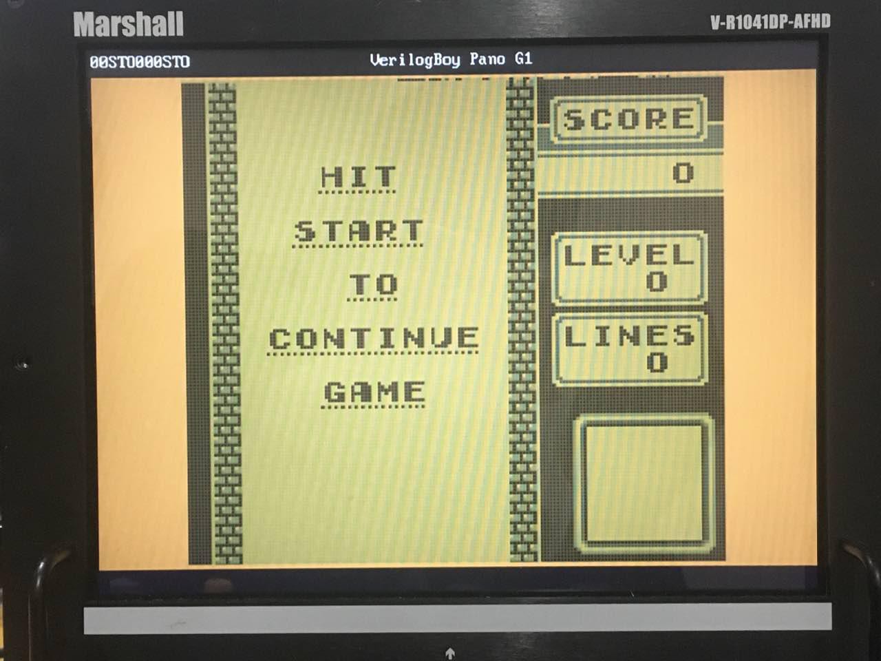
The USB host stack is working, with working USB HID driver and USB Mass Storage Driver
The refactored VerilogBoy CPU is working now, passing all unit tests from the first revision, plus Blargg's CPU test.
These two together, means there are some games actually running on the machine:
![]()
I am planning to do a writeup about the USB, and in the future maybe unit test, but currently, most important:
I will be doing a demo of VerilogBoy at VCF SE during Apr 27-28 and LatchUp during May 4-5.
I am also going to give a talk about this project at LatchUp.
So now the top priority for me is to get these things right, means I would probably not have time to write something here. Anyway, thanks for reading this quick update, and hope to see you guys at VCF SE and LatchUp!
-
A detour to Pano Logic G1 (3) - UART & Hard fault
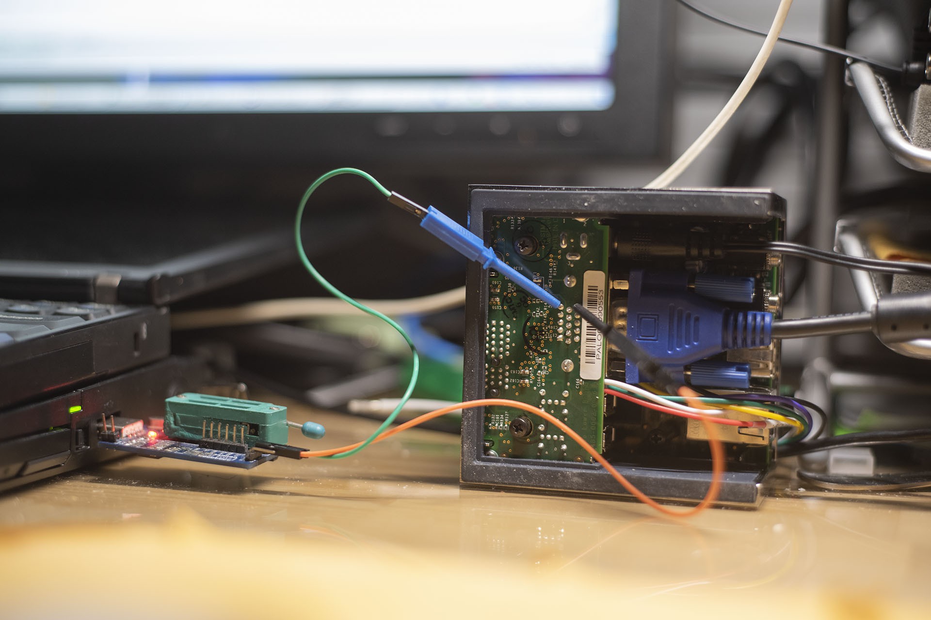
03/26/2019 at 00:40 • 0 commentsIt has been a while since my last update. I have been working on the USB stuff for Pano Logic G1, mainly for connecting to joysticks and flash drives. I was concerned that my LPDDR and cache would cause me some trouble when the code is being executed in RAM, but so far they are holding up well. I will talk more about them in the next log. In this log I would like to talk a little about some debugging utilites, namely, the UART and the hard fault.
UART
UART is very handy when you want to see logs from the device. At first I thought I can get away just by using VGA text terminal, but it soon turns out that 80x30 text is simply not enough. Unfortunately the Pano Logic doesn't have any serial ports. From the schematics, it seems that they originally have one, but was removed after some revisions. But anyway, I have to repurpose the IOs to create myself a serial port to use.
This is not new to Pano Logic, Skip Hansen from PanoMan project has already done this: he soldered a wire to the LED pin and get the serial output from there. For me, as mentioned in one previous log, I do not have soldering iron with me currently, so I need to find some other way.
As an alternate, I used the wire clip come with my logic analyzer. They can be attached to through-hole components easily, such as this VGA connector.
![]()
I am using VGA SCL pin for the serial port. I wrote an extremely simple UART transmitter to transfer the data: https://github.com/zephray/VerilogBoy/blob/refactor/target/panog1/fpga/simple_uart.v. Why I don't just use Skip's UART transmitter core for Pano Logic G1? Or why I don't just work on top of Tom and Skip's project? Well, the (stupid) answer is the same regarding why I picked PicoRV32 rather than VexRiscv: I have decided (long ago) to call this project VerilogBoy, so all the source code should be written in Verilog, not SpinalHDL. Yes I am also aware there are tons of better open-source UART controller written in Verilog available online. I am probably just too lazy to find one considering I don't need other fancy functions anyway.
Using this UART transmitter also very easy, hook it up to the bus and write to the only register available: data register. It has too possible operation modes depending on the way it is connected. If the ready signal is connected to the ready signal of the bus, the UART transmitter would block the code execution until it finishes the transmission. Means the UART print function can be as easy as:
#define UART_TXDR *(volatile uint32_t *)0x03000100
void uart_print(char *str) {
    while (*str) UART_TXDR = *str++;
}
There is no need to worry about if the transmission has finished or FIFO overrun whatever, since it simply throttle the write speed to transmission speed.
Alternatively, if the ready signal is connected to the external interrupt input of the CPU, it can generate a end of transfer interrupt, then a software FIFO can be implemented.
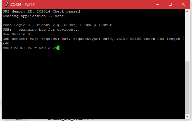
Hard fault
Are you familiar with the Hard Fault in microcontrollers, or Segmentation Fault in Linux, or "The program has stopped working" in Windows? Usually they are referring to the same thing: the code is accessing some memory they shouldn't touch. Most commonly, dereferencing a null pointer (which is nothing more than a pointer points to address 0). I hate this error: they are so common, but not easy to debug. However, I have to admit, it is the one who points out the bug in my code, debugging would be even harder without anyone telling me where goes wrong.
![]()
(It simply hangs when such things happens. It can be hard to determine who caused the issue on real hardware.)
Unfortunately, the processor core itself cannot detect such errors, as it doesn't really know what is right or wrong. Generally, MMU or MPU is in charge of this: the program defines the valid address range (physical address or virtual address, depending on the specific environment.). The MMU or MPU would then generate an exception when an illegal memory access happens. On systems without MMU or MPU, this is generally implemented by the bus controller, accessing to unmapped address spaces would generate an exception. The PicoRV32 doesn't have a MMU or MMU, so I will implement it in the bus.
Sidenote 1: Hard fault on ARM microcontrollers doesn't necessarily mean an illegal memory access. Unaligned memory access, invalid instruction and few other exception will also generate a hard fault. Illegal memory access just tends to be the most common case.
Sidenote 2: On ARM microcontrollers, even if the MPU is not enabled, acessing unmapped memory space would still generate a hard fault, which is nice.
Sidenote 3: I used to implement such a bus controller for 80386, but it didn't work. The 80386 has a prefetch queue, which would blindly fetch instructions after the current EIP. It is very easy for it to fetch things outside of valid memory space. I would assume the same for most modern processors: you probably cannot implement such protections outside of a processor. The PicoRV32 is just simple enough so I am able to implement this.
Codewise, it is trivial: catch all access to unmmapped space, and generate an interrupt.
    reg mem_valid_last;
    always @(posedge clk_rv) begin
        if (!rst_rv)
            cpu_irq <= 1'b0;
        else begin
            mem_valid_last <= mem_valid;
            if (mem_valid && !mem_valid_last && !(ram_valid || vram_valid || gpio_valid || usb_valid || uart_valid || ddr_valid))
                cpu_irq <= 1'b1;
            else
                cpu_irq <= 1'b0;
        end
    end
Inside the firmware, create a hard fault handler,
irq:
# copy the source PC (inside gp register) to argument 0 (a0 register)
addi a0, gp, 0
# call handler
call hard_fault_handler
void hard_fault_handler(uint32_t pc) {
    // External logic is required to connect fault signal to IRQ line,
    // and ENABLE_IRQ_QREGS should be turned off.
    term_print("HARD FAULT PC = ");
    term_print_hex(pc, 8);
    while (1);
}
Don't forget to enable the interrupt at startup:
    // Set interrupt mask to zero (enable all interrupts)
    // This is a PicoRV32 custom instruction
     asm(".word 0x0600000b");
Now try some program that will cause a hard fault, it should fail as expected:
![]()
Sidenote 4: Why I decided to call it Hard Fault rather than Segmentation Fault or Page Fault? Because my system does not have an MMU, so there are no memory pages, it also does not have memory segments as X86 processors do, so it is technically not a Seg Fault or Page Fault. Hard fault is just slightly more accurate. I know I should probably call it bus fault, but that's more like an after thought anyway. It works now so I am just going to leave it as is.
Sidenote 5: Don't put the Boot ROM or anything at address 0. This will make null pointer dereferencing legal and impossible to catch in our case. Guess who is doing that and spent a whole day chasing down some random crash...
Conclusion
Nothing much, really. I implemented both in half a day, just turns out to be helpful for debugging my stupid firmware code. Yes a full JTAG debugger or tracer would be much nicer, but I am running out of GPIOs for me to implement that. I am writting this just to give an update for the project, also sharing some of my ideas. Hope to see you soon in the next update. For the time being, thanks for reading.
-
A detour to the Pano Logic G1 (2) - Cache
03/02/2019 at 16:48 • 0 commentsAs one of the conclusion of the last log, in order to use the LPDDR memory in 32-bit mode on the Pano Logic G1, a cache is almost a must. Sure I can just use 16-bit mode, half the capacity (16 MB) isn't really an issue for me... But I still decided to just implement a cache, it shouldn't be that hard.
So, as a result, I have got cache working on Pano Logic G1. It is a 8-KBytes 2-way set-associative cache. Replacement policy is LRU and write policy is write back. (The whole point of having a cache is because write through is almost impossible given the data mask cannot be used.) It is connected between the PicoRV32 CPU and the MIG memory controller, so all read and writes to the LPDDR is cached. I won't go into details about the cache since I feel like there is nothing special worth talking about except being slow and inefficient. I will add an bus master arbiter between the PicoRV32 and the cache in the future, so the GameBoy CPU could access the LPDDR as well. Though one need to keep in mind this is only a 2-way set-associative cache, having multiple masters would lead to very questionable performance.
So, what about the performance? Currently:
- Read hit: 2 cycles
- Write hit: 2 cycles
- Read miss: 4 cycles + memory read latency
- Write miss: 5 cycles + memory read latency
- Read miss + flush: 12 cycles + memory write latency + memory read latency
- Write miss + flush: 13 cycles + memory write latency + memory read latency
So you can see.. The cost of missing is high, and the cost of flush is very high.
Also, due to my bad coding and the limitation of Spartan-3E's block RAM (it does not support byte enable, which is important for a cache that allows byte enable), compared to 16-bit non-cached version, the whole design uses 1500 more LUTs. I assume mostly comes from the cache, and some from the 32-bit memory controller.
But any way... It Works™.
![]()
How to use:
Make sure g++, riscv32-unknown-elf-gcc, and ISE 14.7 are installed. The RV32 gcc should support march=rv32i.
Clone the VerilogBoy GitHub repo, check out commit b08377d (Merge branch 'refactor').
Run the following command:
cd tools/bin2mif
g++ -o bin2mif bin2mif.cpp
cd ../../target/panog1/fw
make
cp *.mif ../fpga
Go to target/panog1/fpga, open the project pano_top.xise with ISE 14.7 and generate programming file.
-
A detour to the Pano Logic G1 (1) - LPDDR
02/24/2019 at 16:42 • 9 commentsAs I have mentioned in the previous update, I am still having some trouble with the MIPI-DSI. Currently I do not have access to any soldering tools, so the plan of making a new revision of prototype need to be postponed. In the meanwhile, I thought it might be a good idea to continue working on the RTL – I started refactoring the code but haven’t finished yet. But, I need a hardware platform to test. Well, I forgot to bring my FPGA development board (Xilinx ML505, I really loved that board) with me when I came back from Christmas holiday… But no problem, I got myself two Pano Logic thin clients (G1 and G2) last year. Though I have to admit, I didn’t do much with these units after I got them. Now the time has come, let’s take a look.
We have something to hack
![]()
(Image showing is my own Pano Logic G1)
In case you are not familiar with them, let me introduce them first. They were originally thin clients, used to connect to remote desktop servers. What is special about Pano boxes are, they are powered by FPGAs, rather than ARM or x86 CPUs commonly found on a thin client. They advertise it being a “Zero Client”, means there is no (zero) software running on the client. Well, unfortunate for them, they went bankruptcy in 2013. What is fortunate for us is that, these units now become useless for companies originally bought them, being sold for very low price on places like eBay. It is our turn to repurpose these devices! Of course, hackaday has already featured it for several times: https://hackaday.com/2013/01/11/ask-hackaday-we-might-have-some-fpgas-to-hack/, https://hackaday.com/2018/12/07/racing-the-beam-on-a-thin-client-in-fpgas/, https://hackaday.com/2019/01/11/pac-man-fever-comes-to-the-pano-logic-fpga/, and https://hackaday.com/2019/02/11/two-joysticks-talk-to-fpga-arcade-game-over-a-vga-cable/.
![]()
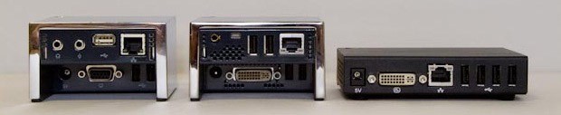
As far as I know, there are 3 generations of Pano Logic clients, the first two looks very similar, and the third is slimmer. Unfortunately I have never seen a slim model on the eBay. If you know anything about the slim model, please tell me, I am interested. The first generation (G1) model is powered by a Xilinx Spartan-3E XC3S1600E FPGA (1600K system gates, translate to around 30K LUT4s.), with 32MB of on-board LPDDR RAM. The second generation model, depending on the revision, is either powered by a Xilinx Spartan-6 XC6SLX150 (Rev. B) or Xilinx Spartan-6 XC6SLX100 (Rev. C), both with 128MB of DDR3 memory. The one I own is a Rev. C one. Both generations has already been reversed engineered by the community, notably cyrozap, twj42, and Tom Verbeure. You may find more information about details of the Pano boxes here: https://github.com/tomverbeure/panologic, and https://github.com/tomverbeure/panologic-g2.Now, which generation should I focus on? Gen 2 is significantly more powerful, however getting harder to find on eBay. The Gen 1, powerful enough for my purpose, and can still be purchased easily on eBay. I decided I want more people being able to play with my VerilogBoy code (if any), so I will go with Gen 1. Also, all the framework I developed for Gen 1 devices might help others looking into playing around with their own G1s.
Talking about the G1...
Then, the gen 1 has already been reversed engineered, someone even published its schematics online, it should be trivial to just port the existing code to the G1, right? No. There are still several issues to be solved:
- The G1 does not have any GPIO for user. In order to attach a game controller, one would need to repurpose some of the IOs (like in the panoman project, he used the I2C from VGA port), or use a USB joystick. Which means I need a host-side USB stack running on a soft core on the FPGA. As I have said, I hope more people can play this, so I will go with the USB solution.
- The G1 doesn’t have any on-board storage large enough to hold the game. The capacity of a typical GameBoy game is between 32KB and 4MB. Famous titles like Pokemon, and Legend of Zelda are around 1MB. The G1 only have a 1MB SPI Flash, and 600KB has been occupied by the bit-stream. Even worse, the G1 doesn’t have a SD or CF card slot, we need to either load the game from ethernet or USB. Well, since I have already need USB for joystick, I will use USB for loading games from.
Now where the games will be loaded to? The only storage element that can hold a 1MB game is the LPDDR memory. At first I thought it is easy to do, I just need to use Xilinx’s MIG to generate a memory controller for me and I just use it as if it is a SRAM, and I have done that before on the ML505. Well, no. The Spartan-3E MIG doesn’t support LPDDR, and the bus width is limited to 16bit (the memory on pano is a 32bit one). And I couldn’t find any open source LPDDR controller core for Spartan-3E online.
Conclusion: I have to make one myself.
So this is what this post all about: making a LPDDR controller for Spartan-3E.
DDR basics
I don't really want to go through all the details about a DDR SDRAM, there are tons of the information online. Here I would just go through some basic stuffs to keep in mind:
- If you ignore the initialization and refresh required by the SDRAM, the protocol is really simple, just like a SRAM, the host sends out the address, and the memory sends back the data.
- Unlike normal SRAMs which use linear addessing, SDRAMs use 2D addressing. The host need to first send out the row address, then the column address. But you may also think it as a linear address, with high bits and low bits transferred at different time.
- Since everything is relatively high speed, delay becomes a thing to consider. Interconnection and logic delay are becoming siginificant relative to the clock period.
- Rise time and fall time, again relative to the clock period, become siginificant. That's why in DDR controller, it is common to manually delay or phase shift the signal, so the clock rising edge is not aligned with the edge of the data, but the center of the data.
- There is a signal called DQS, or data strobe, functioning as a clock for data lines. Usually each byte group of data line would have a corresponding DQS line. This allows the designer to only control the delay within one byte, but not across different bytes.
The Low Power DDR
First, what’s the difference between a LPDDR SDRAM and a DDR SDRAM? Micron has a very nice technical note regarding this: TN4615 – Low Power verses Standard DDR SDRAM. I will just reiterate the main points:
- The DDR uses the SSTL18-I IO standard, while the LPDDR uses the LVCMOS18 IO standard.
- The DDR has internal DLL (Delay Locked Loop), means there is a minimum frequency limitation, the data bus, data strobe and clock are phase aligned; the LPDDR does not have internal DLL, means there isn’t any limitation about the lowest frequency, but the data bus, data strobe and clock are no longer phase aligned.
- The LPDDR has PASR and TCSR functions to help lower standby current.
- Due to the absence of DLL, the initialization process is different from DDR.
For my purpose, only 1, 2, and 4 are relevant to me.
![]()
(Timing diagram showing the difference due to the absense of a DLL)
Where to start?
Writing a DDR controller is all about messing around with delay. One need to careful control the delays between signal to signal to make it work, and input strobe signal need to be delayed for exactly ¼ of a cycle (90 degree phase shift) to be used. On a Spartan-3E, probably the only way to precisely delay a signal is by chaining LUTs together and build an automatic calibration circuit to compensate the temperature change. I am just too lazy to write these myself. So I will start with a working DDR controller and adapt it to work with LPDDR memory.
Then, which one? There are many DDR controllers available online, and few are made for Spartan-3E. I finally decided to use MIG as a starting point. Despite often being criticized for being bloated, the MIG has one important feature: it do latch the data based on data strobe (DQS) signal.
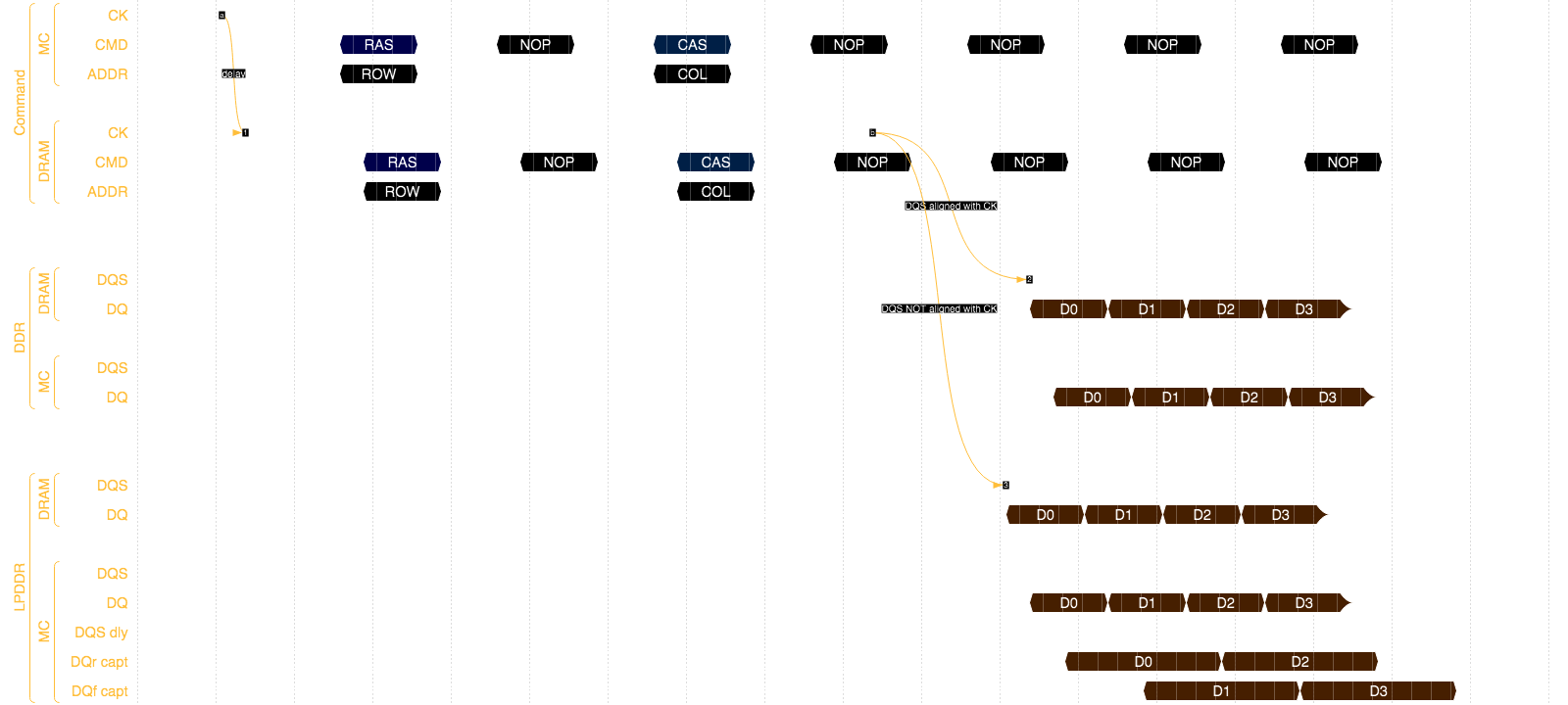
As background information, the DDR memory will output the data and data strobe signal at the same time, and the host should latch the data on the both edges of the data strobe (DQS) signal. And normally, one would want to shift the DQS by 90 degrees, so the edge of the DQS, is the middle of valid data window.
Remember I mentioned the phase relationship issue? Many SDR/DDR controllers are being lazy: they will latch the incoming data based on the internal clock instead of data strobe. This works because, if you neglect the delay, DQS should be equivalent to the DRAM CLK, and that CLK is from the controller's internal clock.
This will bring two important benefits:
First, the whole datapath is now in one clock domain. If one latch the data using DQS, means the datapath would break into main clock and DQS two clock domains.
Second, one no longer need to delay the DQS signal to get a 90 degrees shift, as it is not used for latching the data anymore. Though one still need a shifted internal clock, but that's trivial to do with FPGA's internal DLL or PLL. This greatly simplify the design of the controller.
The downside is basically losing some timing margin, which isn’t a big deal if it is just DDR rather than DDR4. However it is critical here, on LPDDR, there is no longer phase relationship between DQS and clock, the controller has to use DQS to latch data.
The MIG is the only one I found that utilize the DQS, so that is the only choice.
Modifying the MIG
My experience about modifying the MIG is, well, I should say “unexpected”. The adaption is unexpectedly easy, but things break at unexpected places.
First start with modifying initialization process. Well believe or not, this is ONLY modification required to make MIG works with LPDDR! (But other modifications required to just use the MIG)
In MIG, the initialization is handled by a FSM, and it is inside mig_controller_0.v, around line 980. You may check my code here:
https://github.com/zephray/VerilogBoy/blob/refactor/target/panog1/fpga/mig/mig_controller_0.v
Yes, this is all to make the MIG works with LPDDR. However, one would most likely want to also tweak the MIG’s own behavior a little bit, like changing how address bits are arranged (I like make it {row, bank, column} while the S3E MIG default configuration is {row, column, bank}), or changing the parameters (like setting different burst lengths, or CAS latencies).
RISC-V!
Now, the memory controller is here, I probably should connect it to something to test if it actually works. I can use the provided MIG example, it has data pattern generator and will automatically test the controller, but I don’t quite like that approach: it would either tell me success or fail. I would like to know more.
So I decided to connect it to a PicoRV32 soft processor, and use a piece of memory test code to test if the memory actually works. Of course, a simple MIG to PicoRV32 bridge is required to make it work. It is nothing more than a (probably inefficient) FSM. You might see the source code here:
https://github.com/zephray/VerilogBoy/blob/refactor/target/panog1/fpga/mig_picorv_bridge.v
(I will incorporate a cache into the bridge, so if you are seeing the cache and want to check the version without the cache, find historical version of the file.)
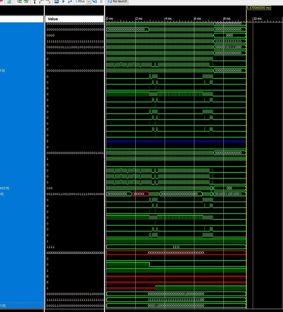
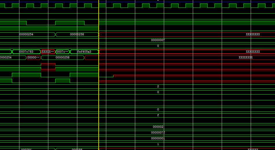
Now, MIG is ready, CPU is in, time to generate the bitstream and test? Well, no. Always do simulation before trying on the board. Micron has provided the LPDDR RAM verilog model, we may just use that and connect it to our board top-level file and run a simulation. Verify the CPU, bridge, and MIG are all working together, and the model doesn’t report any errors.
![]()
(The simulation tells you something even a logic analyzer cannot: Undefined values, undefined would be either 0 or 1 on real hardware and it will be hard to tell.)
Simulation also passed, time to generate the bitstream? Not yet. I still need to write the constraint file.
Design Constraint - From behavioral simulation to the actual FPGA board
First is the definition of all the IO pins for the LPDDR. As I have mentioned before, LPDDR uses LVCMOS IO standard rather than SSTL-I, means we are no longer able to use DIFF-SSTL-I IO standard for differential clock pins, and the differential clock has to be driven as if it was two single ended signals. Well, that’s not a big deal here, we just get rid of the MIG’s differential clock buffer, but use two implied single ended OBUFs instead:
assign LPDDR_CK_P = clk_100;
assign LPDDR_CK_N = clk_100_180;
And just FYI, I have tried using DIFF-SSTL-I for the clock signal on LPDDR, no success, non of the data read back was correct.
Since the DDR controller is so timing sensitive, more delay related constraints need to be added to the MIG. Luckily, Xilinx has provided them. Start by copying the example ucf file to the project and add it to the project. Remove everything related to the board, as they are described in our own ucf file. Then, rename signals to match our design.
Try to synthesis and implement the design, if the ISE complains about cannot find something, double check using Post-Synthesis explorer. If it is a reference to a primitive, add a “*” after the path. After fixing all the errors, it should finish the implementation, but with tons of failing timing constraints. We can see it is because the IOB is too far away from the CLB:
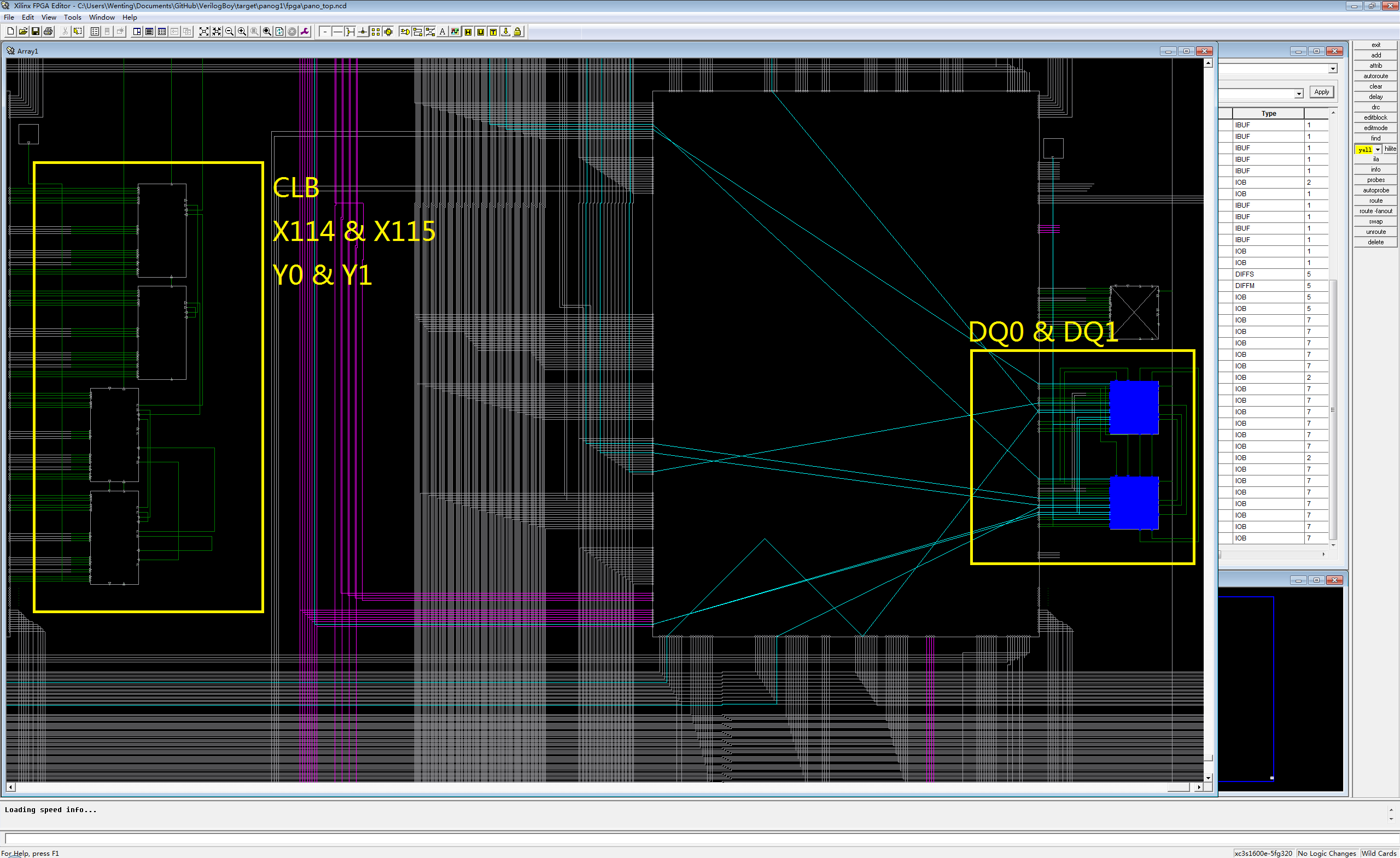
![]()
It’s okay, because we are going to fix that. The idea is that, the delay line and FIFO should be as close to the pin’s IOB as possible. One can find out the closest CLB next to a IOB using the FPGA explorer: find the signal on the right, and see what is the coordinate of the CLB next to it, easy.
![]()
Here is the CLB Y coordinate right next to each DDR signal, I have found them out so you don’t need to do it again.
- DQ0\1 – Y0\1
- DQ2\3 – Y4\5
- DQ4\5 – Y32\33
- DQ6\7 – Y48\49
- DQS0 – Y8\9
- DQ8\9 – Y52\53
- DQ10\11 – Y56\57
- DQ12\13 – Y60\61
- DQ14\15 – Y72\Y73
- DQS1 – Y64\65
- DQ16\17 – Y84\85
- DQ18\19 – Y88\89
- DQ20\21 – Y96\97
- DQ22\23 – Y104\105
- DQS2 – Y80\81
- DQ24\25 – Y100\101
- DQ26\27 – Y116\117
- DQ28\29 – Y144\145
- DQ30\31 – Y148\149
- DQS3 – Y140\141
Go back to the UCF. See all the locations assignments? Well you probably do not need to touch anything related to calibration, they are independent of the datapath and can be located at anywhere inside the FPGA. Xilinx decided to put them in the middle of the FPGA. What we care about is the location of FIFO bits and DQS delay line. Now the rule for MIG is:
- DQS delay line has to be right next to the IOB.
- FIFO write address and write enable should be right next to the delay line.
- Individual FIFO bits may located near by, but don’t have to be right next to DQS or DQ IOB.
Change the site allocation for related primitives and run the Implementation again, now hopefully timing constraint will all pass.
Testing on the hardware
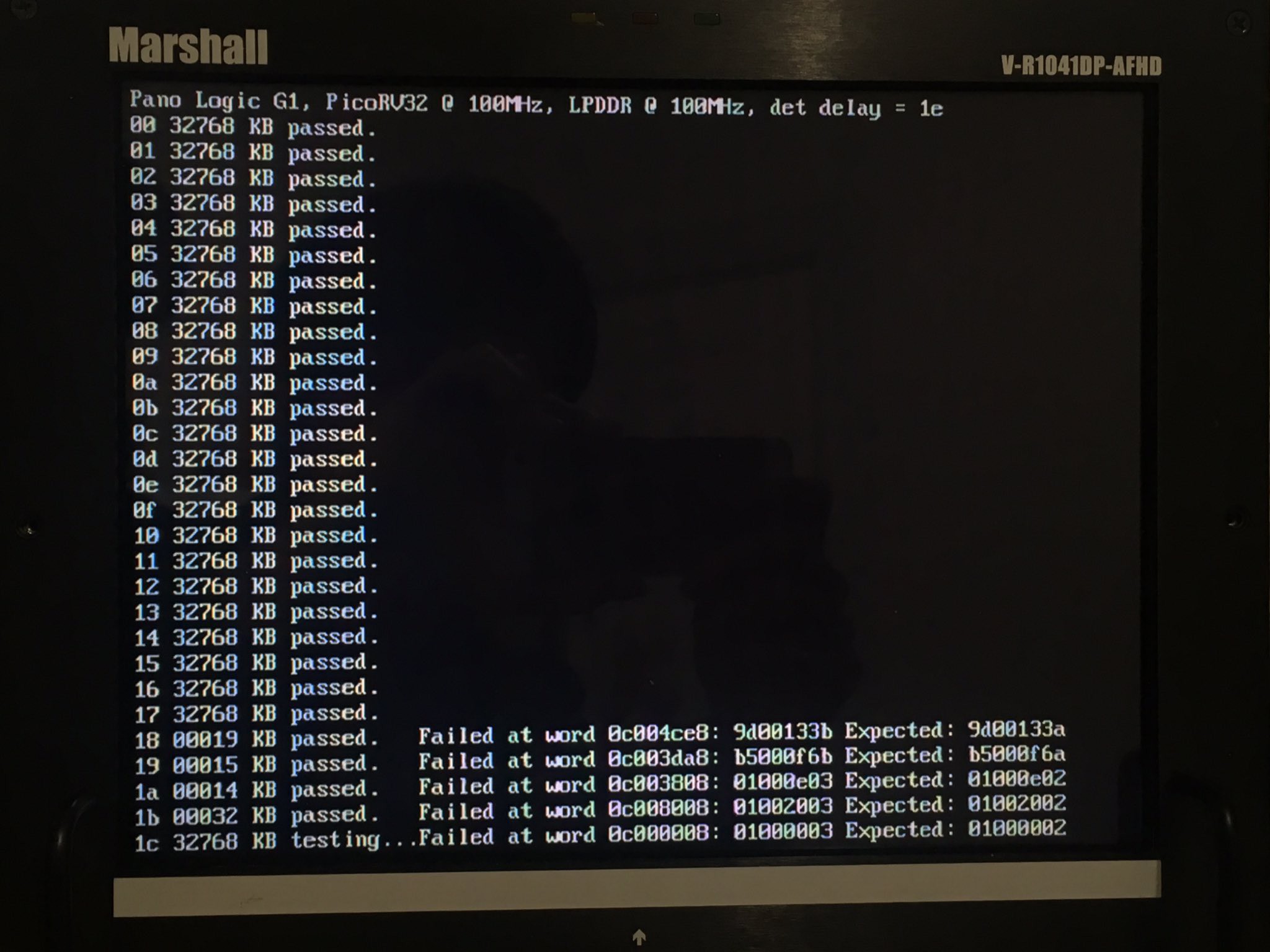
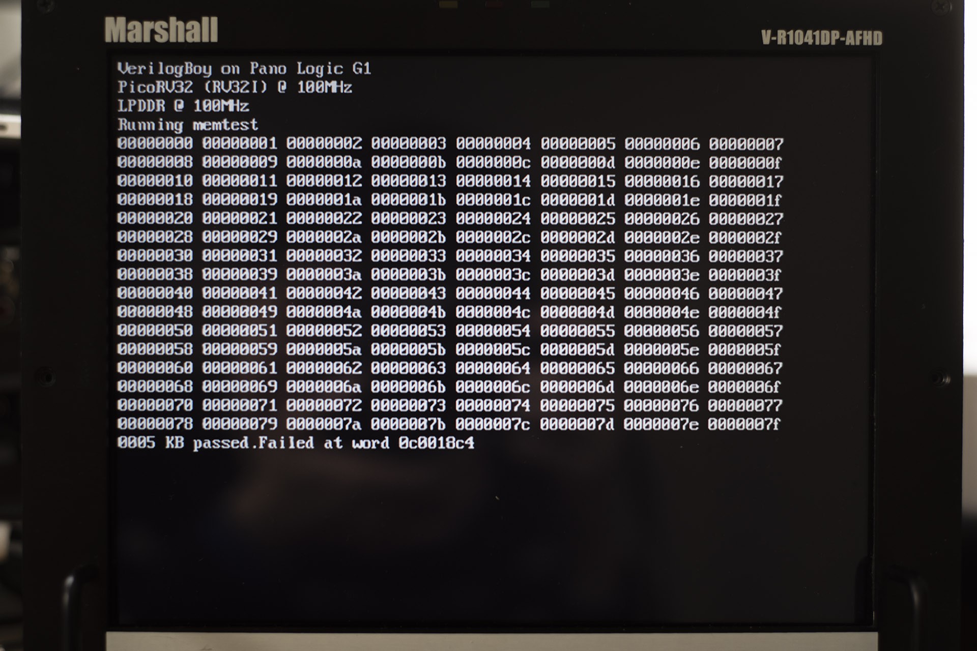
Finally it is time for a test! Well I will be surprised if it works the first time… And the result is:
![]()
Interesting. It is *mostly* working if you say the data is mostly correct, or *mostly* not working if you say it is basically guarenteed to fail within 1 second.
Well, it took me one day to debug the whole thing, here I am just jumping to the conclusion:
There are at least 4 ways I am aware of that can potentially fix this problem:
- The problem may be caused by incorrect delay line tap setting, means the data might be latched too early or too late. Though the Xilinx has a calibration circuit that should determine the best tap value, it is not working for me. It is reporting higher value than it really should be.
- If you see consistant bit error, try adjust the FIFO bit site allocation, it may or may not help.
- If you see consistant bit error and previous method doesn't help, try to ajust the delay of that specific bit, you can adjust the delay value inside the IBUF for that specific bit. By default they are all set to zero. (If you want to decrease delay of that bit, increase the delay of all other bits, and increase the DQS delay).
- Set SLEW for all LPDDR IOs to FAST.
As a result, I used combination of 1, 2, and 4. Don't forget to incorperate a more complex test pattern to test the DRAM. I also write a program to cycle through the different delay tap value to see which works the best:
![]()
You can see anything from 0x00-0x17 is working. This is with slew rate set to fast. If it is slow, only delay value 0x01-0x04 are useable.
MIG Goes 32bit
Now the 16bit mode is working, what about 32-bit?
Though only 16bit mode is supported on Spartan3E MIG, the MIG itself is capable of handling 64-bit memories on Spartan-3 and 3A. After all it is the same MIG. Simply edit the mig_parameters_0.v to enable the 32-bit support:
`define   DATA_WIDTH                               32
`define   DATA_STROBE_WIDTH                        4
`define   DATA_MASK_WIDTH                          4
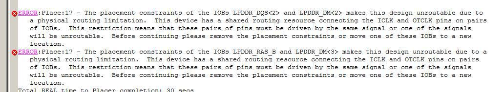
Add constraints of data and DQS lines, modify the PicoRV - MIG bridge to support 32-bit mode, and ready for a test... Then ISE will tell you the real issue:
![]()
What is going on?
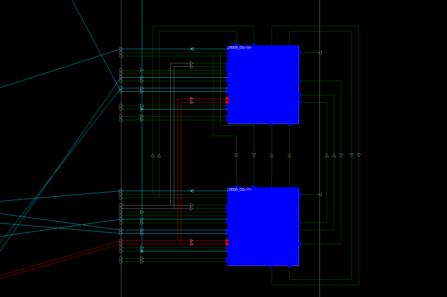
Basically, two IOBs (a pair of IOB) share two same clock lines:
![]()
Means, in such a pair, no more than 2 clock lanes should be used to output the data.
Normally, if it is two SDR signals, one IOB can use one clock lane, and there won't be any conflict at all. But if it is a DDR signal, the IOB would need two clocks (original clock and 180 degree shifted clock) to work. So in a pair, IOBs would either use the same clock (like in the screenshot above), or only one signal can be used.
On the Pano Logic, DM0 and DM1 are in the same IOB pair, so they work together nicely. But for whatever reason, this is not the case for DM2 and DM3, they share clocks with other signals, one is DQS, another is RAS. DM and DQ signals uses 90-degree and 270-degree shifted clock for output, while the RAS uses 0-degree clock. In case of such a pair, 3 clocks are required, and it simply won't work.
Workaround: forget about the DM signals, tie them to the ground. DM (data mask) signals are used to mask out the unused data bytes, so they would be ignored by the RAM. It is used when you want to write less bytes than the minimal transfer length (For 32-bit LPDDR memory, it is 8 bytes, but the MIG can only support down to 16 bytes.), so if we always write all the bytes in a transfer, data masks can be ignored.
But the PicoRV32 works with 32-bit (4 bytes) transfers, how to "expand" it to 16 bytes? The answer is cache. I guess that's out of the scope of this log, so I will continue on the topic of cache in the next log.
Before that, we can still use the PicoRV32 to test the 32bit version of controller, by only write and validate 4 bytes every 16 bytes as a workaround. This would test the 32-bit interface, but limit the useable capacity down to 8MB. It is really just for testing.
The result, of course, it worked.
Conclusion / Take aways
- The LPDDR controller is working, under both 16-bit and 32-bit modes, @ 100MHz.
- Looking at the current timing report, I think 100MHz is really already the upper limit.
- A cache is almost a necessity if you want to use the LPDDR under 32-bit mode. To avoid using a cache, stick with 16-bit mode.
- Source code: https://github.com/zephray/VerilogBoy/tree/f546e0789a65e48243175fab955df40a9778f3e6, under target/panog1 folder. This is for the 16-bit mode. Feel free to copy anything you need.
One more thing...
Do you have a Pano Logic G1? If so, help me test this LPDDR controller! The bitstream is here, simply download it into your G1, and tell me if it works. Failing on some values are expected, as long as it success on few values it is a success. More detailed reports like a screenshot and ambient temperature would be very appreciated. Thank you!
https://cdn.hackaday.io/files/576602466925440/pano_memtest.bit
-
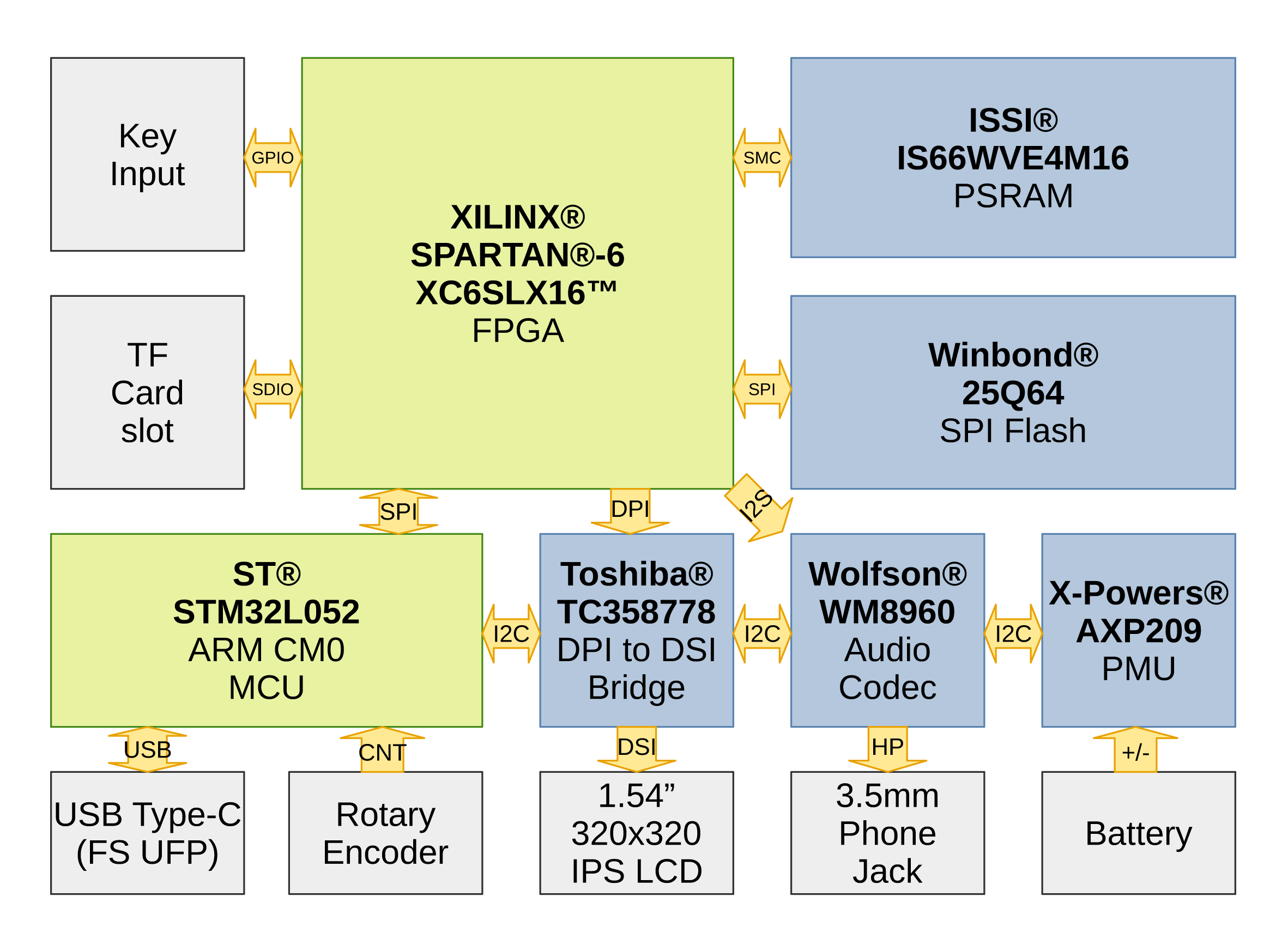
Revised handheld hardware architecture
02/02/2019 at 14:36 • 3 commentsThis is a project update about the hardware side of the VerilogBoy Handheld.
After testing the previous prototype (Rev 0.1), I feel like several changes are required:
- Add a dedicated DPI-to-DSI bridge chip. My poor implementation of the D-PHY transcevier simply couldn't meet the signal integrity requirement. This is an experimental change to test how much it can improve without doing major change to the board (for example, moving to 6-layer, adding decoupling capacitors that would interfere with overall structure, etc.).
- Replace the Micro-Type-B USB socket with Type-C socket. No Alt Fn or PD support is planned, just working under USB 2.0 FS slave (sink) mode.
- Add a microcontroller to handle hardware initialization, RTC, and USB FS communication (for example, flashing new firmware to the on-board SPI flash.
- Fix various incorrect component footprint.
Here shows a revised hardware architecture. This is probably overly complicated for a hobby project.
![]()
Due to the closure of PCB manufacturers because of the Chinese New Year, we are probably not going to see the new prototype (Rev 0.2) in the Feburary. I will continue working on the HDL side of the prototype and trying to finish the CPU refactoring within the coming weeks.
For the time being, thanks for reading.
-
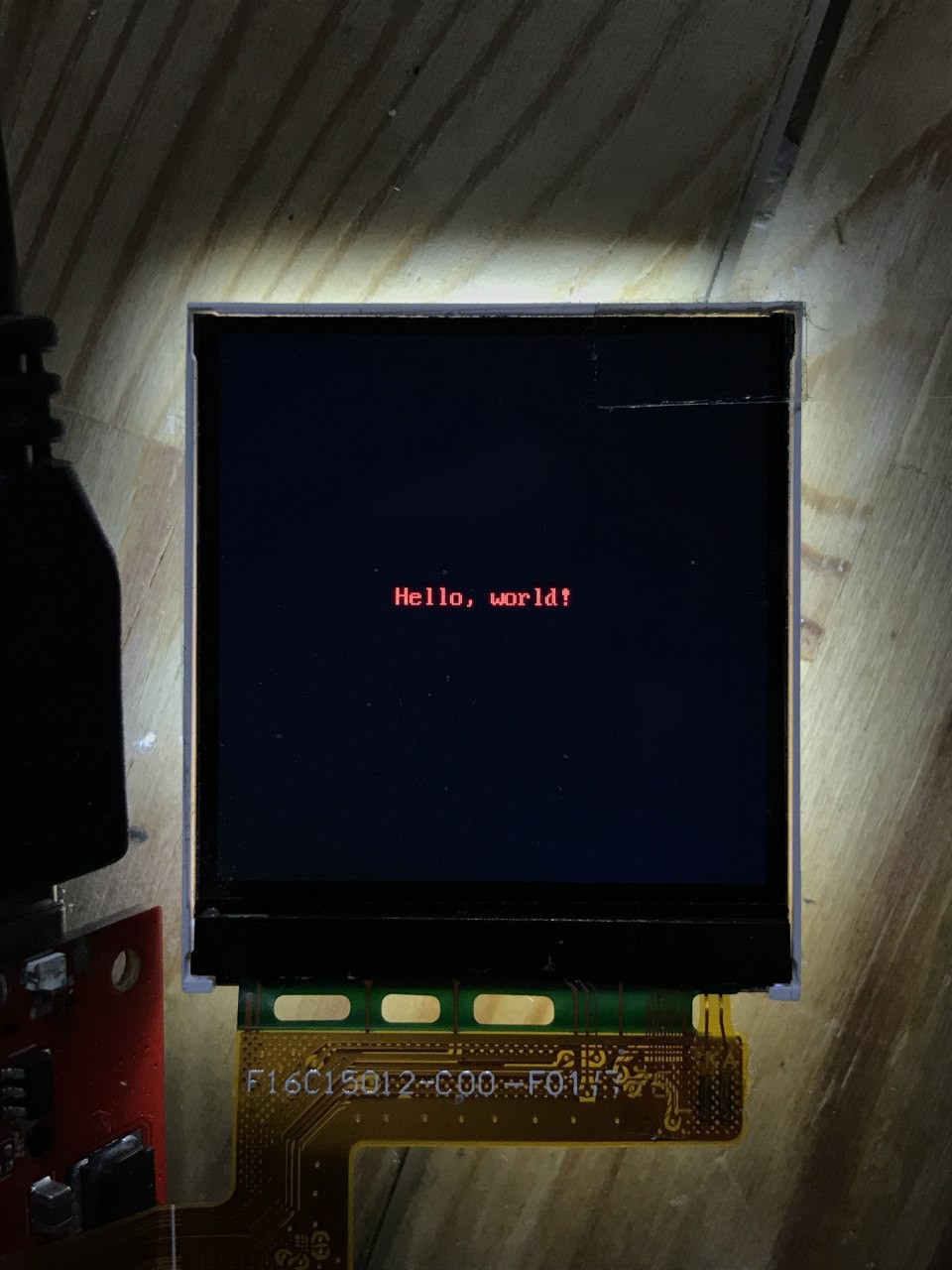
Hello from the DSI screen
01/28/2019 at 17:41 • 0 comments![]()
Here it is. 320x320 IPS MIPI DSI screen. DSI running at 268 MHz (256 MiHz), that's exactly 64 times the Game Boy pixel clock rate (4 MiHz). With every GameBoy pixel quadrupled, and every pixel being 16 bits (FYI, the GBC uses 15bpp), it is going to transmit the pixel output from the PPU to the screen perfectly in sync. DSI controller is implemented in FPGA. A custom boot ROM running on the GameBoy CPU takes care the DSI controller initialization as well as screen initialization. More details about DSI is coming. -
The Assembled PCB.
01/14/2019 at 02:11 • 1 commentUnfortunately due to the system design, I have to finish refactoring the CPU first before I can do some practical tests (which all need the BootROM to run on the CPU within the FPGA). But, at least, here is a nice looking board!
![]()
VerilogBoy - GameBoy on FPGA
A Pi emulating a GameBoy sounds cheap. What about an FPGA?
 I promised that there would be an update about the USB, here it is. This update would only talk about the USB 2.0 Host on the Pano Logic G1 devices with ISP1760 USB host controller, so it is probably not applicable to other platforms. The goal here is to write a set of RTL and software stack, so it is possible to use USB HID joystick/ gamepad and USB mass storage devices on the Pano G1. Speed would not be the concern here.
 What are these? Is there always one embedded hub in the controller? Not really. The host driver sometimes needs to control the port. For example, turn on or off the power supply of a specific port, or reset a specific port. For USB hubs, they are implemented as control packets sent to the USB hub, the hub would receive these packs and function accordingly. But to control ports on an EHCI compatible controller, one would need to use MMIO to modify certain registers to accomplish the same thing. From the driver interface perspective, this is inconvenient: there would be two different interfaces to do the same thing. As a result, generally in the HCD (host controller driver), there would be some code to emulate a hub: it would intercept control packets sent to endpoint 0, reports itself as a USB hub, and write values to MMIO when certain control packets are being received. So there would be a third hub in the system. Imagine our poor packet would have to go through at least three hubs before it can reach the other end… And our protocol stack must be able to handle multiple layers of hub as well.