 Kumar, Abhishek
I could sit gloating over my toner transfer results but I knew it wasn't going to help too much as I had to assemble my boards. So there were a few more steps:
(i) Manual "HSL" treatment - Coat the board with flux and then use the angled bit of my soldering iron to tin all the traces serving the dual purpose of protecting the copper from tarnishing and filling up any etch imperfections in the traces.
(ii) Drilling all the vias and connecting them - this is where the board fab wins hands down over home PCB fabrication. Also learning how difficult it is to use carbide bits and not break them. Used some single strand wire to fill the vias and cut them flush to the board surface after soldering. Then manually checking each and every connection with a multimeter to ensure they tunneled through the layer gap..
Okay, once all this is done, then apply solder paste on the pads and place every component manually. Then a quick reflow with a hot air gun.
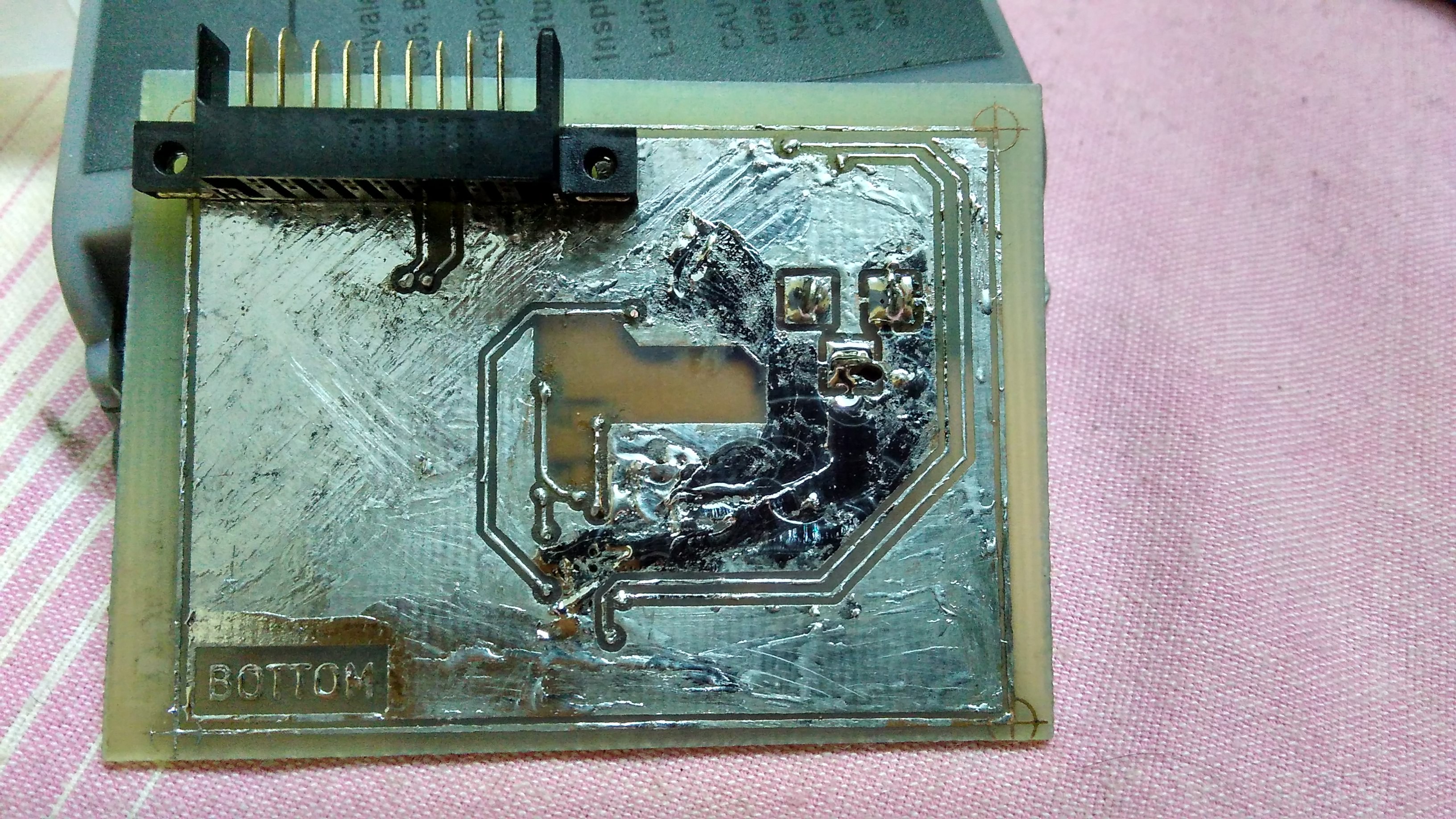
Then solder the two through hole components - the barrel jack and the battery connector (on the other side)
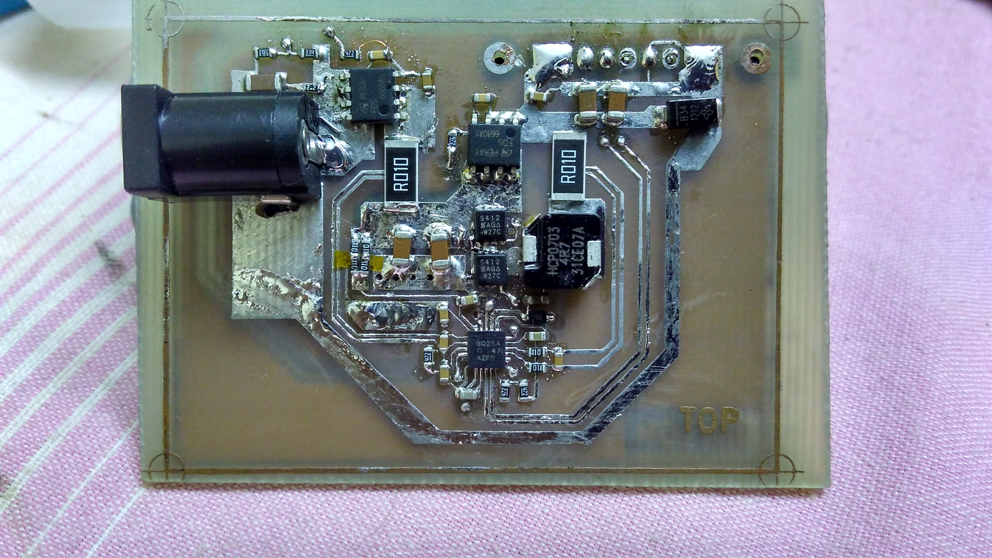
Yes, it is very difficult to do solder-levelling on large filled copper areas.
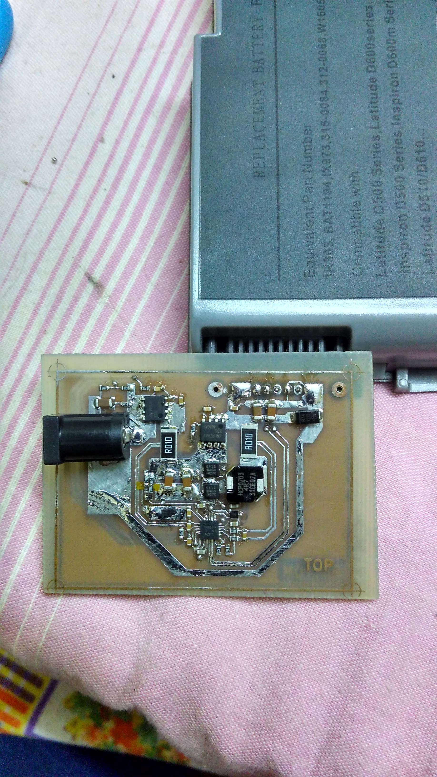
Attached on the battery:
Discussions
Become a Hackaday.io Member
Create an account to leave a comment. Already have an account? Log In.
On 'drilling with carbide tips: I've done 'freehand' and 'drill press', and will never -EVER- go back to freehand. Just that much easier/happier.
Are you sure? yes | no