Close
0%
0%

YoctoBob - a BOB for an ultra tiny Cortex M0 proc.

NXP has released a Cortex M0 processor in a tiny BGA 16 package. Why not design a cool break out board for this device.

Similar projects worth following
The NXP LPC1102 is perfectly suited for small wearable sensors and data loggers. I plan to design an ultra tiny 3 axis acceleration logger that will be embedded in a shuttlecock (!). First step will be to test the design thanks to a "large scale" mock up.

A break out board for this processor will surely speed up the integration tests.

Main features of the LPC1102

  • ARM Cortex-M0 based processor
  • 32-bit MCU
  • CPU frequency up to 50 MHz
  • 32 kB on-chip flash memory
  • 8 kB SRAM
  • 11 General purpose input output pins
  • 10 bit ADC
  • 1 UART
  • 1 SPI controller
  • Internal 12 MHz RC oscillator
  • Consumption: approx 2 mA @ 12 MHz
  • Package: Wafer level chip-size package, 16 bumps, 2.17 X 2.32 X 0.6 mm

This device is currently one of the smallest Cortex M0 based processors available on the market.


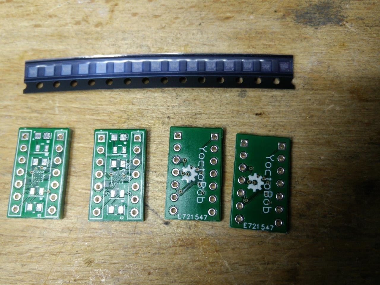
Aspect and pinout of the YoctoBob module
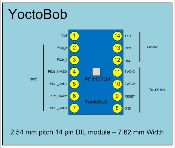
(Pinout updated on 2015/05/24)


MCU pin allocation

Bump Pin designation YoctoBob Pin number YoctoBob Pin designation Remark
D2 VDD 1 VDD Power Supply
A2 PIO0_8/MISO/CT16B0_MAT0 2 PIO0_8 GPIO
A3 PIO0_9/MOSI/CT16B0_MAT1 3 PIO0_9 GPIO
B4 R/PIO0_11/AD0/CT32B0_MAT3 4 PIO0_11/AD0 GPIO
B3 R/PIO1_0/AD1/CT32B1_CAP0 5 PIO1_0/AD1 GPIO
C4 R/PIO1_1/AD2/CT32B1_MAT0 6 PIO1_1/AD2 GPIO
C3 R/PIO1_2/AD3/CT32B1_MAT1 7 PIO1_2/AD3 GPIO
D3 VSS 8 GND Power Supply
C1 RESET/PIO0_0 9 RESET Programmation
A4 SWCLK/PIO0_10/SCK/CT16B0_MAT2 10 SWCLK Programmation
D4 SWDIO/PIO1_3/AD4/CT32B1_MAT2 11 SWDIO Programmation
B1 VSS 12 GND Power Supply
C2 PIO1_6/RXD/CT32B0_MAT0 13 RXD Console
D1 PIO1_7/TXD/CT32B0_MAT1 14 TXD Console
A1 VDD N/A
B2 XTALIN N/A

(Table added on 2015/05/17)

  • "Manufacturing" tests (2015/09/04)

    Michel Kuenemann09/17/2015 at 01:26 0 comments

    I have purchased a bunch of LPC2102UK processors (15) and carried out soldering tests on several PCBs.

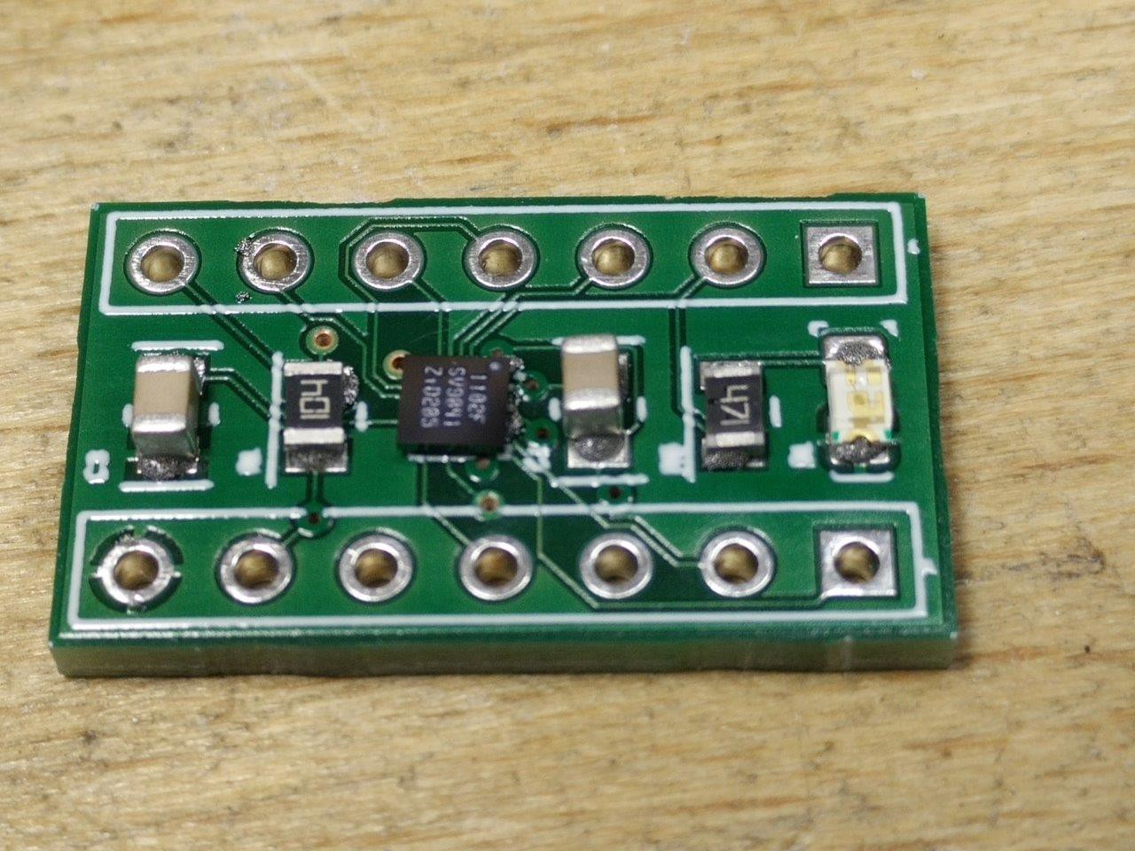
    I used a reflow curve suited for leadless solder paste. After the reflow process, the BGA device was correctly placed on its landing pattern. The following picture shows one the boards. On this example the device is correctly placed, but there is some solder coming out on the right side. On this board I added some leaded soldering paste on the pattern before reflow with a syringe - It was not a good idea at all. Other boards did not have this issue.

    I made several soldering tests on 4 boards and I tested the boards that seemed OK. The consumption of each board was very low (less than 1 mA). I connected the boards to my LPClink probe and tried to flash a program. I did not manage to flash the program in any of them.

    Here are my findings:

    • After the reset, the I/Os of the micro should be pulled-up to 3.3 V and I found that all of them were close to 0 V.
    • The SWDIO and SWCLK wires should also be pulled to 3.3 V - They were also close to about 100 mV.
    • The RESET wire had a correct steady state level (3.3 V)

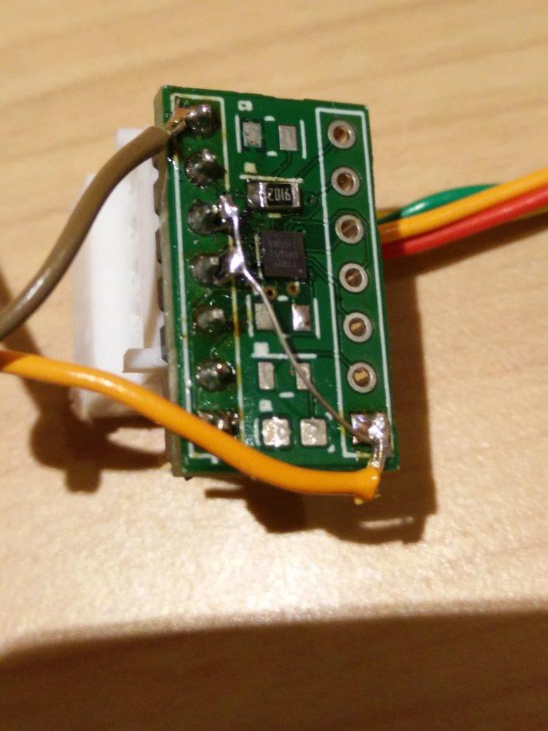
    On the following picture, I even added pull-ups on SWDIO and SWCLK to "help" the programming process but it did not work.

    Conclusions:

    Positive points
    The correct positionning of the device on the pattern is not very difficult to achieve. I had no device "drifting" during the reflow process. The size, the pinout and the general concept of the board are really cool and nothing should be changed regarding these aspects of the project.

    Negative points
    I think that the pads are too small to achieve a correct electrical contact. Despite of all my efforts, I did not manage to get even a single board working. In a new version, we should try to increase the BGA pads diameter. Maybe we can find a (maybe chinese) manufacturer who will provide boards will small clearances at low cost.

View project log

Enjoy this project?

Share

Discussions

Frederik Dubois wrote 05/21/2015 at 13:49 point

Do i see via directly in the BGA pad? This is a big no-no IMHO, they'll suck the solder righ in the hole and you won't have a good contact between the ic and the pad or not at all. Unless you plan to do fully copper filled via?

  Are you sure? yes | no

Michel Kuenemann wrote 05/21/2015 at 13:55 point

Hello Frederik,

Thank you for the feedback. We are aware of this issue and we are currently discussing it with Merkourios. We would like to have this PCB manufactured by Eurocircuits, with their standard pool process in order to optimize the cost.

Do you think that it is practically possible to:

* fill the vias with melted solder paste, 
* remove the excess of tin with a solder wick,
* put some flux,
* place the BGA,
* reflow

Keep in mind that we just want to produce 2 or 3 boards for evaluation.

Regards,

Michel

  Are you sure? yes | no

Frederik Dubois wrote 05/21/2015 at 15:22 point

With the standard pool at Eurociruits you have access to 4mils traces (0.1mm Min. track width/spacing), can you fanout the inner four balls directly on the top layer by routing them between outer balls and place your via outside the IC? The outer 12 balls can be routed without placing via directly in the pad, just move them couple of mils on the outside.

You don't have any 0401 or 0201 Capacitor on the bottom side directly under the bga chip for the vcc, so there is no reason to not use traces on the top layer to help you fanout the signals properly given the fact that you can use 4mils traces.

It's lot less trouble to not mess around with filling via then soldering the bga package than it is to fanout properly in the first place!

If you have access to an X-ray scanner you could be able to easily check if all the balls are correctly soldered after your technique of pre-filling the vias, but I don't know a lot of people who can afford that!

I may be wrong, but i'm just trying to help based on my experience!

Fred

  Are you sure? yes | no

Michel Kuenemann wrote 05/21/2015 at 15:31 point

Hello,

Thanks for your very relevant advices. We will discuss them. If we can avoid these vias in the middle of the balls with 100 µ traces, we will do it !

Regards,
Michel

  Are you sure? yes | no

[deleted]

[this comment has been deleted]

Frederik Dubois wrote 05/21/2015 at 15:52 point

I wasn't sure if it was possible with the inner four, thanks for clearing that up, there is at least the other 12 that can be routed without vias.  For the inner 4, do you have enough clearance to place each via in the middle space of a 4 balls square? btw, you solder mask expansion seems to be large around the balls pad?

  Are you sure? yes | no

[deleted]

[this comment has been deleted]

Frederik Dubois wrote 05/21/2015 at 16:05 point

Hi,  have you contacted the fab house about that? They can sometime reduce their OAR if they can add a proper teardrop to the via, it happened to me last year on a 0.4mm bga chip, it helped me a lot. 

If not, i read somewhere that to reduce the amount of sucked solder, you can tent the via in the bottom layer so that the air pressure inside the via blocks solder from being sucked in.

  Are you sure? yes | no

Michel Kuenemann wrote 05/21/2015 at 18:13 point

Hello Merkourios and Frederik,

I have a (maybe stupid) suggestion: 

why not "cheat" and reduce (a little) the diameter of the pads to comply eactly with the rules ?

Michel

  Are you sure? yes | no

[deleted]

[this comment has been deleted]

Michel Kuenemann wrote 05/21/2015 at 19:14 point

How much would it be necessary to reduce the pads to be 'just" compliant with the rules ?

  Are you sure? yes | no

[deleted]

[this comment has been deleted]

Michel Kuenemann wrote 05/21/2015 at 19:45 point

So, do you confirm that with 0.2 mm can we avoid the vias in the balls ?

  Are you sure? yes | no

[deleted]

[this comment has been deleted]

Michel Kuenemann wrote 05/21/2015 at 20:12 point

Tell me if I am OK :

Assuming 150 µ diameter balls (very small balls), it would be possible to fanout a 100 µ trace with 125 µ clearance, so avoiding the very very bad vias in the  internal balls.

(150/2) + 125 + 100 + 125 + (150/2) = 500 µ ( = pitch)

On the other hand, 150 µ is half of the minimal recommended diameter, so it will be, maybe, much more difficult to have a good soldering. The question is: which is the "best" solution - Vias or very small balls ? My opinion would be to test the small balls first...

Is this reasoning correct ?

  Are you sure? yes | no

Frederik Dubois wrote 05/21/2015 at 20:42 point

Hi both of you,

Yes your reasoning seems fine!

I can't choose for you, but you also have to keep in mind that you have to align this chip to solder it correctly (you'll see 2mm by 2mm it's very very small between your tweezer's tip). My guess is that you'll be positionning it by hand? The precision alignement will be produced by the surface tension of the molten solder and the flux, but if you reduce too much your pad, the force applied by the surface tension will also be less and could result with a misaligned ic..!   

I think the fab house will be more than happy to help you with that issue by giving you tips or a footprint recommendation, you're certainly not the first ones to try a chip scale BGA with 0.5mm pitch!


  Are you sure? yes | no

Michel Kuenemann wrote 05/21/2015 at 20:53 point

Thanks a lot for your contribution, Frederik,

I am sure we'll learn a lot from the supplier - Let Merkourios ask them for support.

We'll keep you updated.

Regards,
Michel

  Are you sure? yes | no

Michel Kuenemann wrote 05/24/2015 at 14:53 point

Hello Frederik,

Merkourios managed to design the PCB in accordance with Eurocircuits' rules. The BGA pads have a diameter of 150 µ. We have ordered 10 boards for delivery by beginning of June.

We will keep the project log updated.

Regards,
Michel

  Are you sure? yes | no

davedarko wrote 05/18/2015 at 10:47 point

spotted a mistake in your pinout diagram :) instead of a 7 there's a 3. But the rest is awesome :)

  Are you sure? yes | no

Michel Kuenemann wrote 05/18/2015 at 10:51 point

Hello,

Thanks a lot for your proof reading. I will correct this typo ASAP.

My colleague Merkourios is currently designing the board. I hope that a first schematic issue will soon be available on the repository.

Michel

  Are you sure? yes | no

Michel Kuenemann wrote 05/20/2015 at 16:01 point

Hi,

Drawing is updated.

Regards,
Michel

  Are you sure? yes | no

suicidal.banana wrote 05/18/2015 at 10:22 point

Love the idea, just hope you can manage to solder that thing. (Actually, anybody know any tuts on soldering BGA parts? or is the general consensis still to just add wires to it?)

  Are you sure? yes | no

Michel Kuenemann wrote 05/18/2015 at 10:47 point

Hello,

Yes, soldering the device will be tricky. I saw some tutos on YT showing that, thanks to the balls, it is not necessary to put soldering paste on the PCB. So I will try to put some flux on the pcb, place the device and put-it in my reflow oven. I will use leaded solder paste. Due to the low pin count of the device, I hope I will get one or two good boards among 10...

Michel

  Are you sure? yes | no

suicidal.banana wrote 05/18/2015 at 15:17 point

Ah, ok, well let us know how that goes, would be interested to hear :)

  Are you sure? yes | no

Gilles KREBS wrote 05/16/2015 at 20:58 point

That microcontroller sounds really cool!! I like your project!!

  Are you sure? yes | no

Michel Kuenemann wrote 05/15/2015 at 18:16 point

Hello,

That thing is really sexy indeed.  Thanks for following.

Michel

  Are you sure? yes | no

zakqwy wrote 05/15/2015 at 18:13 point

Wow that thing is tiny! Wicked cool!

  Are you sure? yes | no

Similar Projects

Does this project spark your interest?

Become a member to follow this project and never miss any updates