 peter jansen
The revised high energy particle detector boards arrived, and I've had the chance to put one together and verify it working over the weekend — and snapped some pictures of the assembly process along the way. This (long!) post details the assembly process, and (towards the bottom) describes some initial characterization of the detector, including a histogram of detector variability.
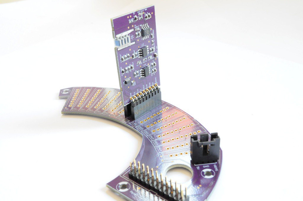
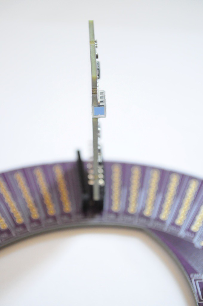
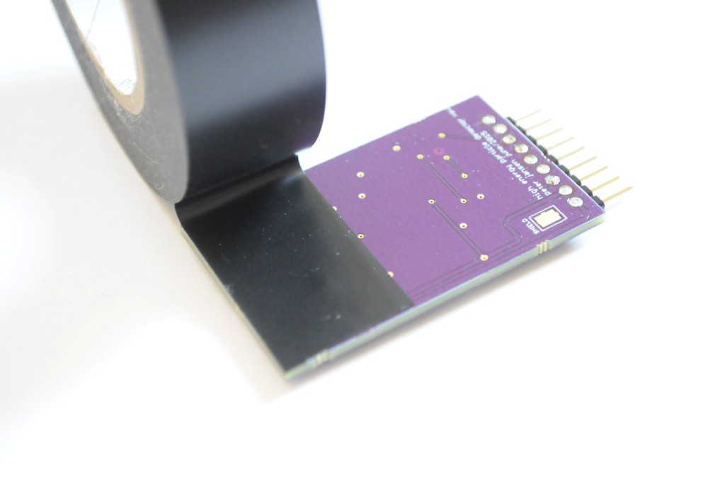
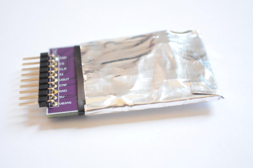
Pictured above is one of the Radiation Sensor Revision 1 boards, coupled with the very curiously-shaped Imaging Array board. It’s not often that I find myself having to design boards in interesting shapes, and while the first goal is of course to design something that works, it’s always wonderful when you have the opportunity to make it look aesthetically pleasing, too.
Assembly
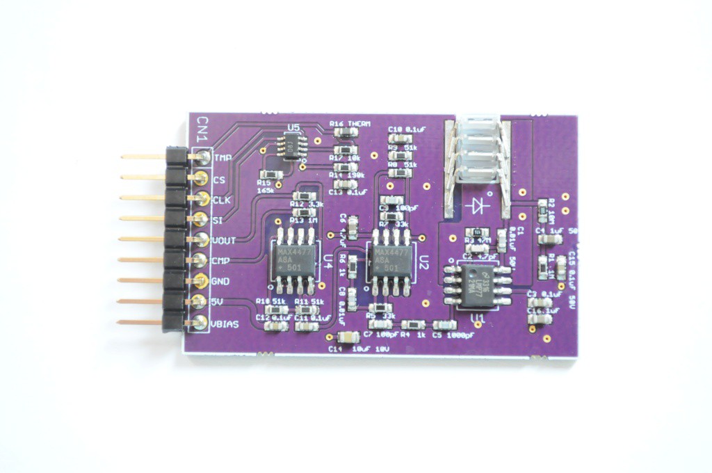
The Radiation Sensor Revision 1 designs are available on Github, including the schematics, gerbers, and parts list. The boards I’ve shown have been ordered from OSH Park, and the stencil from OSH Stencils. Most of the component values are included on the board silkscreen, so it’s generally a comfortable assembly process if you have experience assembling a few surface mount boards. (Note that the detector I've assembled here has had C2 changed from a 4.7pF to 2.2pF to examine if a higher gain on the first stage significantly improves signal to noise, but so far it looks like either value should work just fine).
In addition to the normal surface mount soldering process, there are a few additional steps in the assembly process to accommodate bending the photodiode leads, creating a light-tight wrap, and applying the grounded shield. These are a bit atypical, so I’ve documented them here.
Photodiode Angling/Stacking Jig
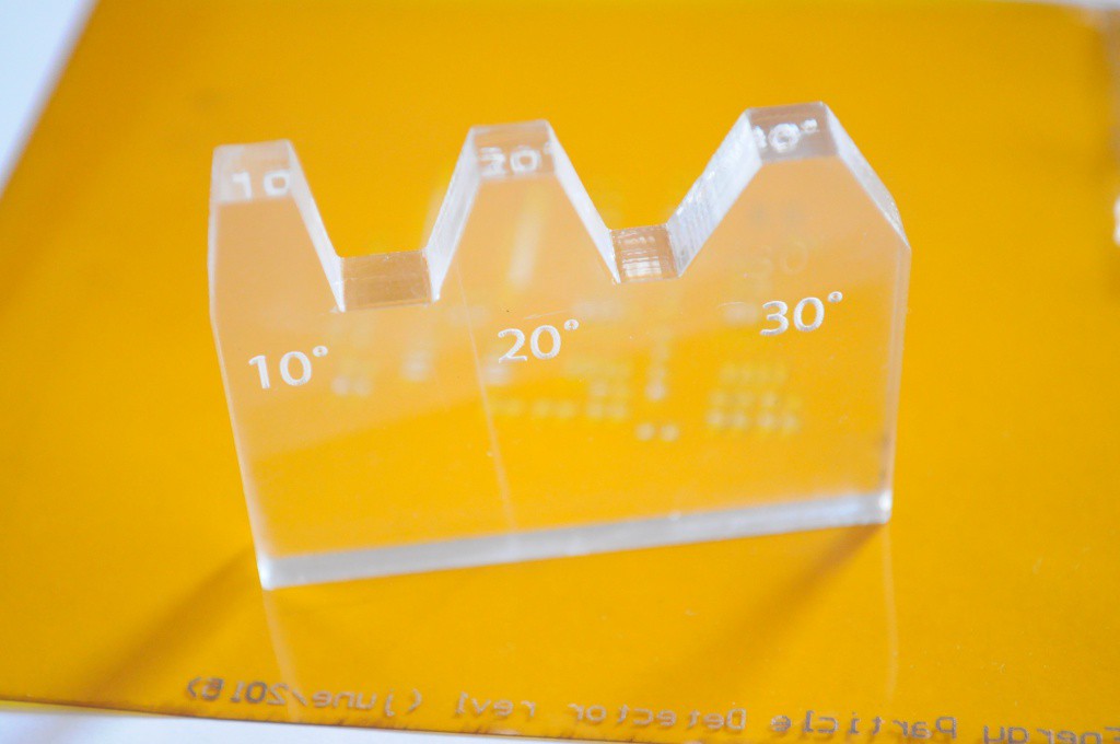
The detector uses an array of four BPW34S photodiodes stacked one atop each other (and, laying on their side) to dramatically increase detection efficiency. Straight out of the tube these photodiodes generally come with leads that are 90 degrees from the main body, and need to be slightly angled so that they easily sit atop one another (and make contact with the surface mount pads on the board).
A small laser-cuttable jig to perform this bending is available here, and pictured above. The jig contains 10, 20, and 30 degree pin angles — I find that the 20 degree works optimally. To bend the photodiode, lightly squish it onto the jig, and the pins will spread to the appropriate angle. I have found that 3/16″ acrylic worked well for this jig, being about the same width as the photodiode.

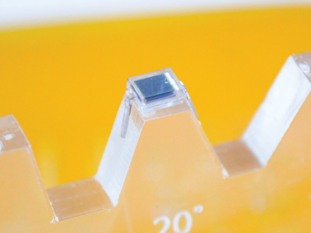
Above we can see the difference in between the original pin angle (left) and pins angled slightly at 20 degrees (right) to enable stacking. I recommend that the photodiodes be the last components placed on the board, using tweezers, and sitting (laying?) flush one atop another.
Connector Lead Trimming
To get as high an imaging resolution as possible and increase the packing efficiency, the detectors have been designed to be as thin as possible — only 4mm (!) on the imaging dimension. To ensure that they’re as thin as possible, the main 9-pin male connector (bottom) may need to be slightly trimmed, depending on the part you use.

(The imaging array board for the “cat” scanner, with an actual cat, for size).

The connector that I’ve spec’d for the radiation sensor boards is Digikey #S1111EC-09-ND. I looked for a connector with the shortest leads that I could find, and confess that from the datasheet I had expected the pins to be a little shorter. Normally you could use a surface mount connector for this and not have to deal with through-hole leads poking out of the back of the board, but the alignment of our imaging array is important, so I’ve included the through-hole connector with slightly offset pins to encourage the connector to align properly. I’m also convinced that the through-hole connector is likely more mechanically stable than a surface-mount version.
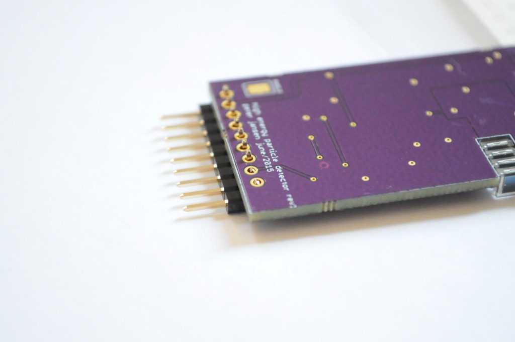
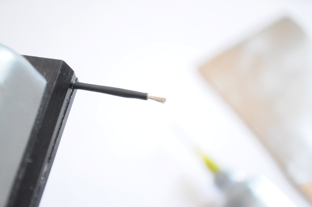
Here (above) we can see the start of the pins being trimmed — either a standard pair of wire trimmers or right-angle trimmers should work well for this.
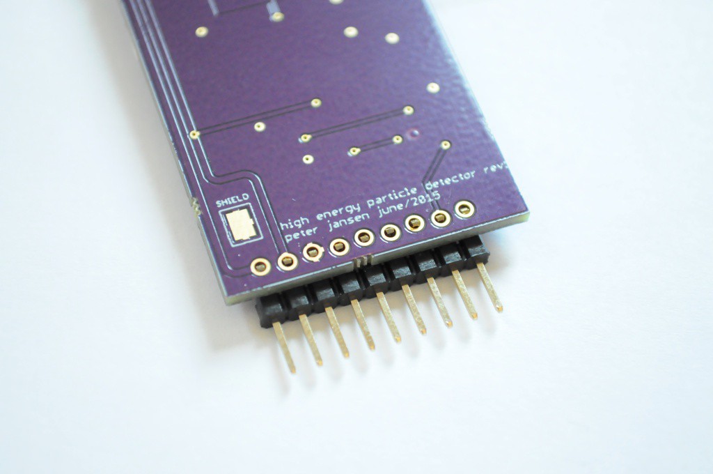
And here each of the pins has been trimmed. When soldering, don’t forget to warm up the pin before applying the solder — it’s important to encourage the solder to fill the hole from top to bottom, and be both mechanically rigid and a solid conductor.
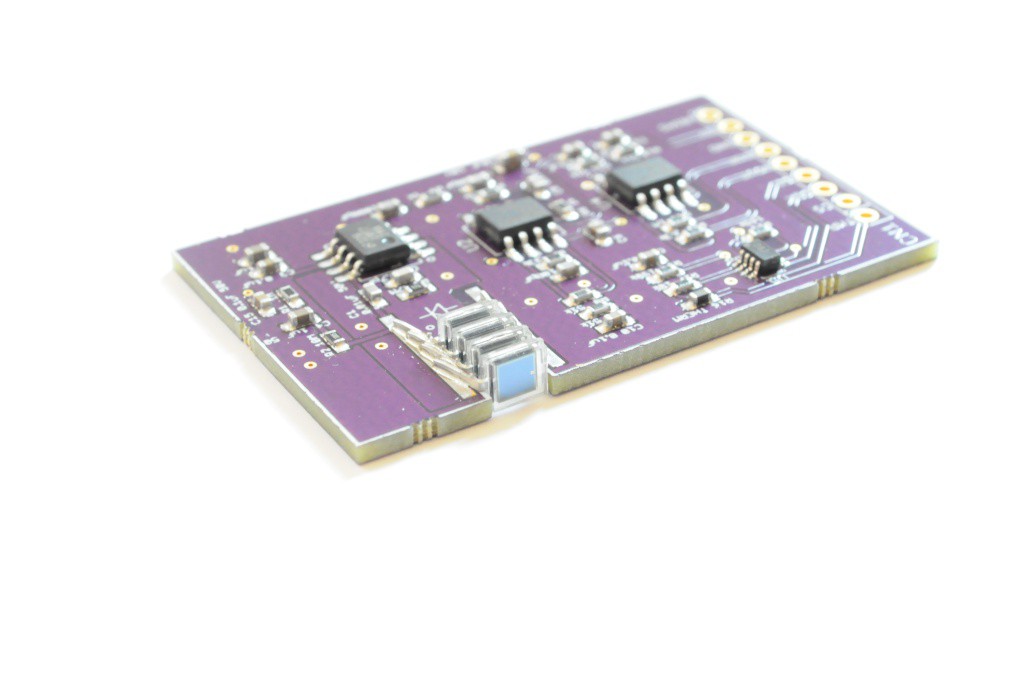
The board, after soldering on the connector. Ready for wrapping!
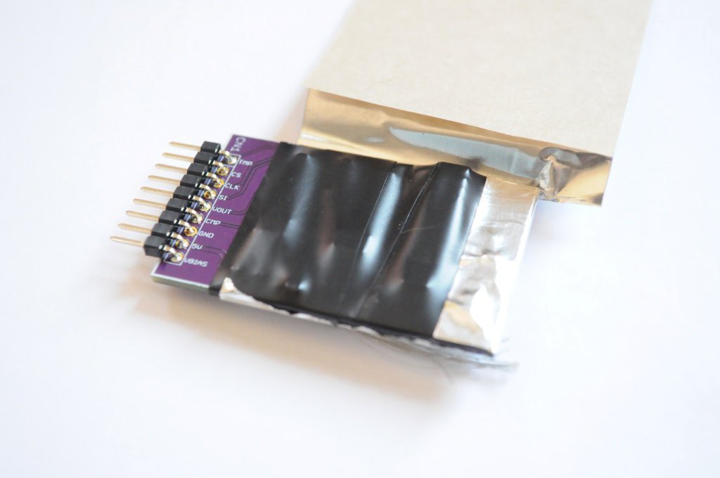
Wrapping Part 1: Insulating light-tight layer
The detector has to be wrapped in several layers — both to shield the photodiode from any external light, and provide a grounded conductive shield to reduce the electrical noise. I do the wrap in two layers — a layer of black electrical tape (to shield from light, and insulate the board from the conductive tape), then a layer of aluminum tape for the grounded shield.
Here, I prefer to start at the the top of the back of the board…

Then wrap around the front, completely covering the photodiode stack with a single layer of electrical tape. From here, I wrap around the back again…

… and several more times, until the entire board (including all parts and vias) are covered, save the connector at the bottom, and the “shield” pad on the back of the board at the bottom (below). I try not to cover the bulk of the photodiodes in more than one layer of electrical tape, so that the photons don’t have more bulk material to go through before hitting the photodiodes (not that the electrical tape is likely to be terribly absorptive).
While the top (component side) of the board will be a little bumpy from all the components, try to wrap the back side of the board as smoothly as possible, as we’ll have a mechanical ground wire connection to place here in a moment.

Wrapping Part 2: Grounded Aluminum Shield
The second layer is a wrap of Aluminum tape that surrounds the detector and provides a grounded electrical shield that reduces electrical noise. This is a critical part of the circuit, so take your time to ensure that the shield is well crafted.
The first component of the shield is the ground wire (above). Cut a piece of stranded wire about 1.5 inches in length, with a small section stripped at the bottom, and a much larger section stripped near the top. Pre-tin the bottom section, but do not apply any solder or twist the large stripped section at the top (this will make sense in a moment).
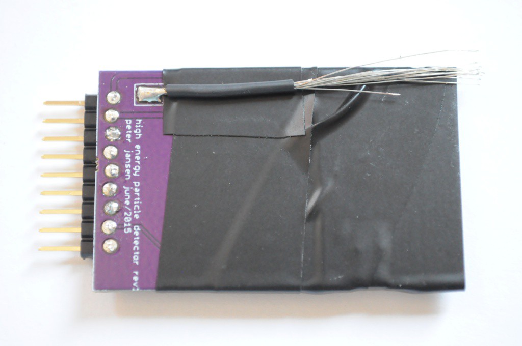
Solder the ground wire to the ground pad on the back side of the board. I recommend holding the wire down with another piece of electrical tape (while soldering) to ensure that it’s as flat to the circuit board as possible. We’re about to cover the back of the board in aluminum tape, so try to ensure that the back is as flat as possible.
We can’t solder the ground wire to the aluminum tape, so we have to make a solid mechanical connection. The method that I’m showing here is what I’ve inferred is likely used with the Radiation Watch Type 5, after carefully examining it.
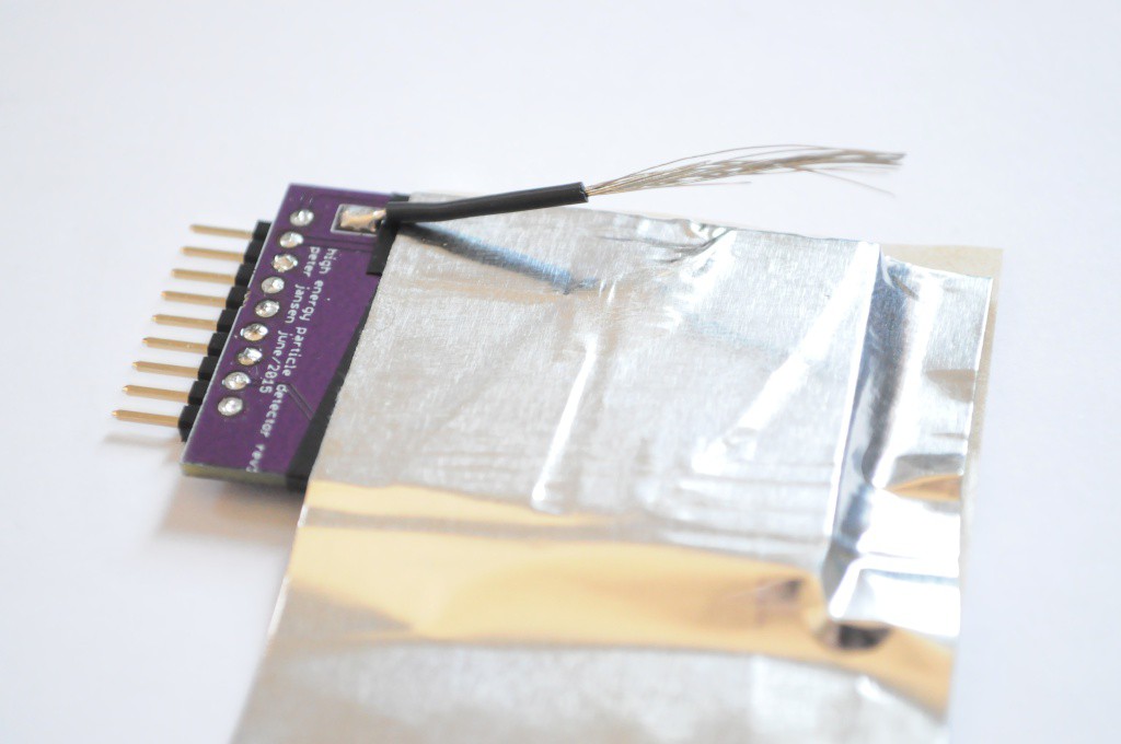
Cut a piece of aluminum tape that’s about three times as long as the detector is wide (~10cm). The aluminum tape I use is standard off-the-shelf tape from Home Depot intended for sealing ventilation conduits.
Make the first layer on the back of the board (as shown above), aligned with the edge of the board on one side, and just above the shield pad/electrical tape on the other. Remember, ensure that the electrical tape covers /all/ components and vias with a margin of a few millimeters, and ensure that the aluminum tape is seated completely on the electrical tape (with a bit of a margin) and not touching the board — otherwise it may bridge and cause a short circuit!
It’s okay (and preferred) for the tape to extend over the top of the board a little — just cut a seam along one edge,…
… and bend it over the top of the board, as above.
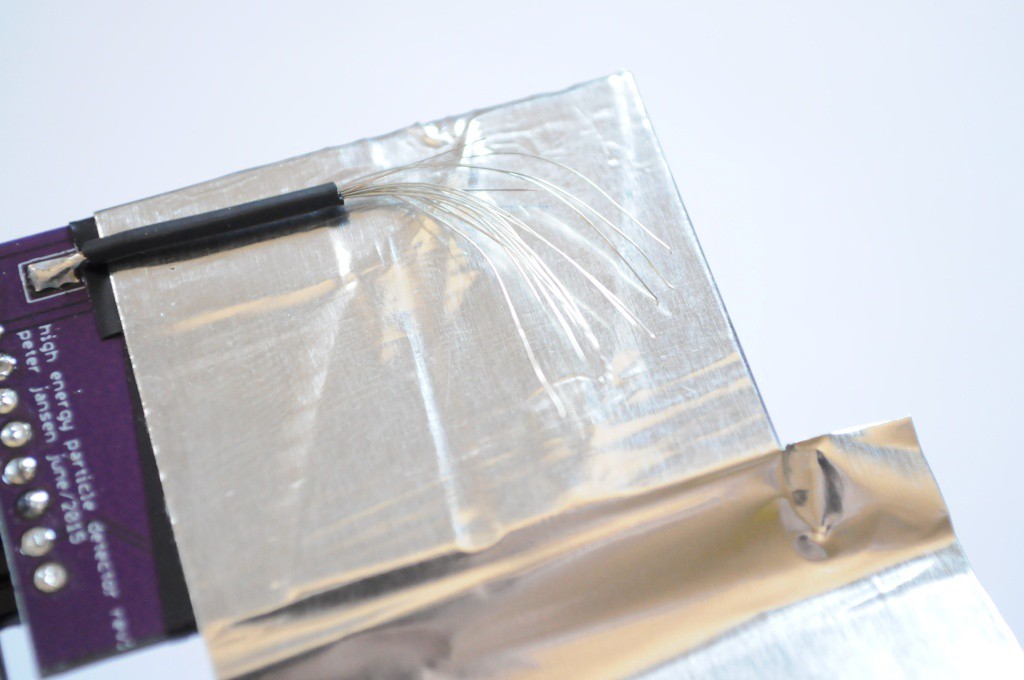
Place the board in a board vice, and carefully fan out the stranded wires over the back of the board, as above. The idea here is that they will be sandwiched between the conductive layer of aluminum tape below them, and the adhesive layer of aluminum tape we’re about to put overtop of them.
Note that the more stands we have in the stranded wire, the better the connection is likely to be. The wire that I’ve spec’d for this (Digikey #CN100B-25-ND) is 22awg 17 conductor strand wire, which has many more strands than the cheap 7 strand wires, and should perform much better for this task.
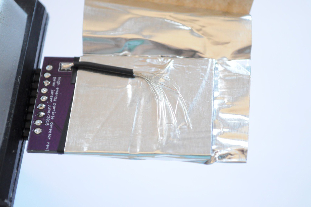
Wrap the aluminum tape over the front of the board. For the excess tape over the top, again cut a small slit along the seam, and fold the excess down onto the top of the board.
Now the critical fold — slowly fold the tape over the back (and the bare stranded wire), ensuring that it’s reasonably tight, and squished down such that the stranded wire is very firmly pressed into place against the underlying layer of aluminum tape. Use a meter to verify that the aluminum tape shield is effectively grounded.
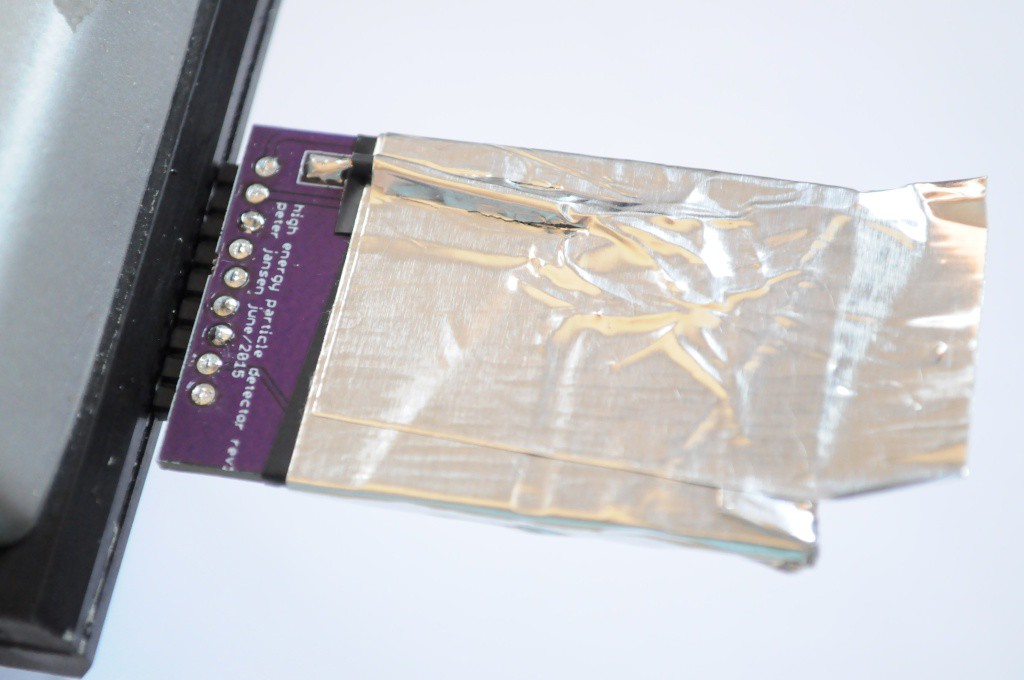
And, lastly, fold any excess over the top of the board. Congratulations, the board should be light-tight, and electrically shielded! Don’t forget to use a meter to verify that the shield is grounded, and that there aren’t any electrical bridges between the shield and any of the pins on the connector.
Performance and Measurement Variability
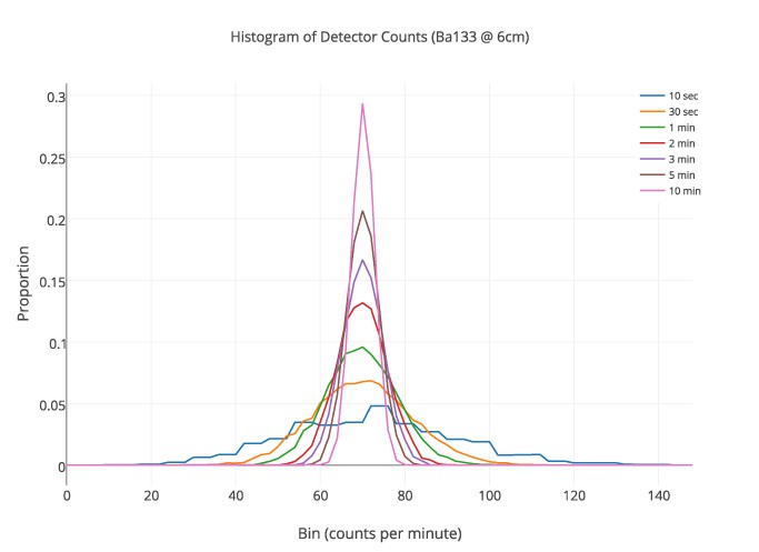
In terms of general performance, with the 10uCi Barium-133 radioisotope source ~6cm away from the detector, the detector measures an average of 70 counts per minute (cpm).
Absorbance imaging from a weak radioisotope source is an interesting problem — if you think of another (simpler) example of absorbance imaging, holding up a film negative or slide to a lamp, assuming the lamp you’re using to backlight the slide is fairly uniform, it’s easy to make out the picture on the slide. With weak radioisotope imaging, the source is fantastically more dim, and so instead of having an enormous stream of photons backlighting the sample, we’re essentially counting single photons as they interact with the detector, about one per second. On timescales of minutes to hours the average rate that the Ba133 source emits these photons is about constant, but on the shorter timescales that we’re using for imaging, there’s much more variability (a phenomenon known as shot noise). For imaging, this is further complicated in that x-ray photons are being emitted from the source in all directions, but each pixel is very small — at a 6cm radius around the source, a sphere has a surface area of 45,238mm^2, but each detector is sensing photons from only 7.5mm^2 of that sphere (a difference of a factor of over 6,000), so there will be quite a bit more variability in our measurements. But how much?
Above I’ve plotted a histogram that helps illustrate the measurement variability using a technique called Bootstrap Resampling. Here, I’ve connected up an Arduino Uno to the detector, and set it to listen for detections for 10 seconds, and report the detection rate (in cpm). I then do this many times over the course of about 2 hours, until there are nearly 1000 of these 10 second measurements, and plot them as the blue line in the histogram. Here we can see that there’s quite a bit of variability in these short measurements — they span from about 20cpm, when few photons happened to be emitted in the direction of the detector over a given 10 second interval, to 140cpm, where there was a photon party in detector town, and everyone was invited. The bulk of the measurements show rates of between 40-100cpm, with a roughly Gaussian distribution. (For those interested, the raw data is available here, and the histogram is available on Plotly).
To simulate the variability at integration times longer than 10 seconds, I use bootstrap resampling to randomly draw a number of 10 second samples, and average them. For example, to simulate a 20 second integration time, one would randomly draw two 10 second samples, and average them. To simulate a minute long integration time, one would randomly draw six 10 second samples, and average them. If you do this random resampling many times — here about 10,000 times per integration time, then you can simulate a smooth distribution.
| Integration Time | 10s | 30s | 1m | 2m | 5m | 10m |
| Standard Deviation | 20.3 | 11.7 | 8.4 | 5.8 | 3.7 | 2.6 |
Here we can see both on the histogram and in the table (above) that on timescales of tens of seconds, the variability is quite large compared to the average rate (over long timescales) of 70cpm. For those not familiar with statistics, the Standard Deviation is a measure of variability in a Guassian-shaped distribution. The measured value will be between +/- one standard deviation from the mean value of 70cpm about 68% of the time, and within +/- two standard deviations of the mean value 95% of the time.
Here we can see that on timescales of tens of seconds, the variability is quite large — at a sample time of only 10 seconds, we’ll measure a rate of 70 ±20cpm (or 50-90cpm) 68% of the time, and a rate of 70 ±(20*2=40)cpm (or 30-110cpm) 95% of the time. That’s very large, and so such short integration times won’t be very useful for imaging — with such a high variability, the image would look very noisy.
The integration time follows the Poisson relationship, such that measuring for N times longer decreases the variability in the measurement by sqrt(N) — so measuring for twice as long decreases the variability by a factor of about 1.4, and measuring for 4 times as long decreases the variability by a factor of 2. We can see this in the table above, where the standard deviation at a 2 min/120 sec integration time (5.8) is twice as stable as the variability at only a 30 second integration time (11.7). The target (“within the limit of patience”) integration time of 120 seconds means the signal intensity will vary from 70 ±5.8cpm (64-76cpm) most of the time, to 70 ±12cpm (58-82cpm) 95% of the time. This should be more than enough to generate a low-resolution image, and with some filtering we may be able to clean up a bit of the noise in the images as well.
Next Steps
The next step is to put together a partial array of detectors (about 4) to verify their performance and repeatability. If everything looks good, the imaging array can be mounted onto the tomography platform, and we can move towards collecting the first imaging data.
Acknowledgements
I'd like to thank the generous folks at Texas Instruments for sending along enough of their exceptionally low-noise LMP7721 Precision Amplifiers to complete the array.

Thanks for reading!
Discussions
Become a Hackaday.io Member
Create an account to leave a comment. Already have an account? Log In.
I still suggest biasing two photodiode arrays either side of the current sensing amplifier, such that you can give twice the detection area with the same number of amplifiers.
Are you sure? yes | no
I'm not sure that I understand your suggestion -- the purpose of stacking the 4 photodiodes one atop each other is to increase the detection area without sacrificing spatial resolution. If you placed two arrays beside each other, you'd have twice the detection area, but half the spatial resolution?
Are you sure? yes | no