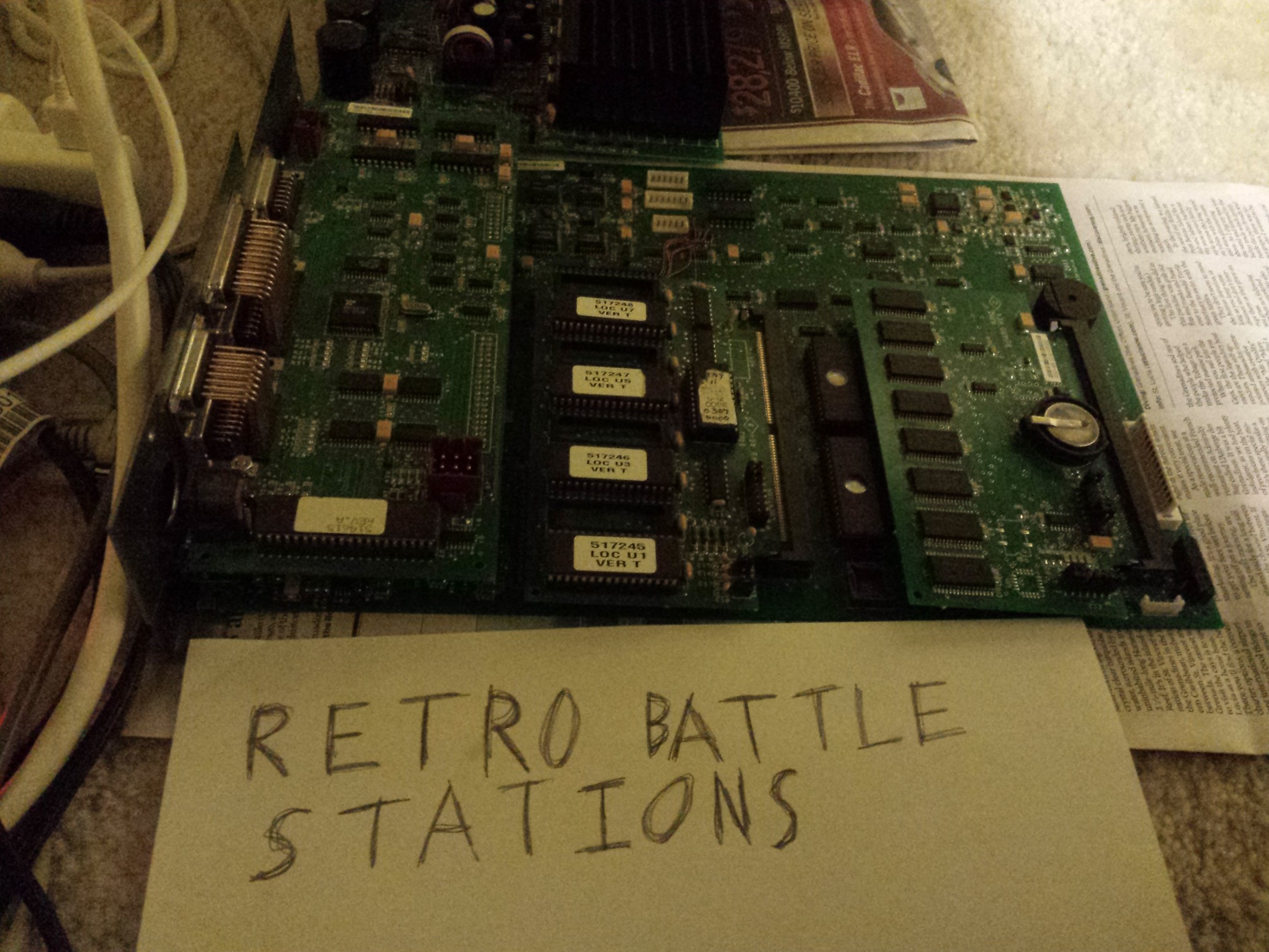
I have been reverse engineering the hardware of this 68332 based system in order to run my own software on it. What that software will be specifically, I don't exactly know yet.
This is a link to all of the pictures:
Note: many of these pictures are quite large, up to about 5MB
Here is copy and paste from the text file I use to document anything I reverse engineer from the hardware:
default setup of address space
this could change if software changes it
$00 0000 - CSBOOT, 1MB, onboard boot ROM
$10 0000 - CS0, 1MB, card 1 & 2, addon ROM card
$40 0000 - CS1, 1MB, card 3 & 4, onboard DRAM
$5C 0000 - CS8, 256KB, card 8, onboard SRAM
$60 0000 - CS2, 1MB, card 5 & 6, SRAM card
$B0 0000 - CS7, 1MB, 8 bit port, videochip
$D0 0000 - CS5, 16KB, I/O
$E0 0000 - CS9, 2KB, 8 bit port
$F0 0000 - CS10, 64KB, 8 bit port, I/O
$FF E000 - TPURAM, 2K
$FF F000 - internal CPU on-chip registers
CS5 controls U210, a 74AC138 for address decode
CS9 goes to a pin on J3, and nowhere else as far as I can tell.
CS10 goes to U25, a 74AC138 for address decode. also goes to pin on JA1 for daughterboard.
hardware I/O addresses:
CS5:0-7FF - UART1
This is the base address for the 68C681 on the mainboard. The base set of registers is repeated to fill the block of addresses.
CS5:802 - LEDS - doesn't clear IRQ
CS5:800 - PPORT - clears IRQ
This write address controls the parallel port output pins and the 4 onboard LEDs. Bit 15, 14, 13, and 12 control CR 50, 51, 52, and 53 respectively. Bit 11 controls the /SELECT_PRINTER line. Bit 10 controls the RESET line. Bit 9 controls the /LF line. Bit 8 controls the /STROBE line. The lower 8 bits control the data outputs. This address is repeated in the range 800-FFF everytime ADDR2 is 0. If any address in this range is read or written which has ADDR1=0 then the /ACK interrupt is also cleared.
TODO: figure out how to read the status lines for the parallel port, should be U57
CS5:1800-1FFF - J4
CS5:2000-27FF - RTC
Base address for Epson RTC registers
CS5:2000-2800 - EEPROM
CS5:3800-3FFF - DRAMC_CNTL
This address is used to write U719 (74AC573), an 8 bit latch. The actual chip seems to have the data lines hooked up backwards from the numbering in the datasheet, and it's attached to the high bits of the CPU data bus. The output of this latch is enabled or disabled by TPU channel 15. A 0 on the TPUCH15 pin on the 68332 enables output from this latch. Bit 6 and 7 appear to be unused. Bit 5 controls the DRAM controller /DISRFSH line. Bit 4 controls the DRAM controller /ML line. Bit 3 and 2 go to the PSU connector. Bit 1 and bit 0 seem to mask interrupt sources from the power supply board. A 1 masks the interrupts. The interrupts share a single interrupt latch flip flop and use IRQ1. They are cleared by a reset or reading this address.
CS7:0-FFFFF - ISA bus/SVGA controller
The SVGA controller is mapped here. 0-7FFFF seems to be mapped to I/O reads and writes (not confirmed) while 80000-FFFFF seem to be mapped to memory reads and writes. This is necessary because the video chip is made to work on an ISA bus which has separate memory and I/O spaces while the 68K does not.
chip is setup for MCLK on MCLK pin
ISA bus
Symmetric DRAM
single WE, multiple CAS
6 MCLK RAS cycle
44.74431MHz MCLK
32K ROM BIOS at C0000-C7FFF
8 bit BIOS ROM
Internal MCLK
3C3h is video system sleep register
CS7:02000-02007, 02406-02407 - ATA registers
This is piggybacked into the pseudo ISA bus used for the VGA controller. Decoding is done using a 74ACT138 decoding the top 6 address lines (A15-A10).
CS10:0-3FF - UART2
This is the base address for the 68C681 on the daughtercard. The base set of registers is repeated to fill the block of addresses. This also reappears at 2000-23FF
CS10:400-7FF - KB controller
odd addresses are status/command, even addresses are data. These registers may be repeated at 2400-27FF
CS10:800-BFF - MTR_CNTRL
This address writes to U18 (74AC573) on the daughtercard. It's bits control various motor functions on the daughtercard. Bit 7 seems to be disconnected by a jumper....

 Samuel A. Falvo II
 TEC.IST
 Anders Dinsen
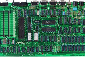
 Keith
Keith
I am looking for the 68K source for ehbasic. If you have a location for it, would you provide a link? Thanks!