 Hayden Kroepfl
Well sometimes it seems like it's working, but it only ever does half of what I expected. My initial attempt at getting visible output has been to use the A23 pin to blink an LED. I've gone through various iterations of the code, fixed bugs such as not have the the supervisor stack pointer in the ROM before the starting address. The problem I keep getting is yes the led blinks, and it even does it's pulses at seemingly the right time compared to the address strobe, but I can't control the rate at which it pulses. In the code I'm counting down d0 while writing to an address with A23 high, then I toggle A23 in the address and repeat the cycle. The problem being that changing the starting value from the count never affects the pulse rate. Another odd behavior noticed is that all the other address lines above A18 pulse at the same rate which makes little sense, they're all just floating (adding a pull down doesn't change it though) and the code is writing to address $840000 which should not be touching them.
    ORG    $0

    DC.l $0043000        ; Supervisor Stack Pointer
    DC.l start           ; Initial PC
start:
    movea.l #$840000, a0 ; Address of the first byte of ram
                         ; But with A23 set so it's written to LED
loop:
    move.l #10000, d0
delayloop:
    subi.l #1, d0
    move.b d0, (a0)
    cmpi.l #0, d0
    bne.s delayloop

    move.l a0, d1
    eori.l #$800000, d1
    move.l d1, a0

    jmp loop
In the picture below you can see what I mean by it seeming to work, the top row is the ~AS line, every time it goes low there's a valid address on the bus, the second is the ~chip select for the RAM, and the third the ~chip select for the ROM. It kind of makes sense there being 4 ROM accesses, then a RAM as the RAM is getting written to one in the loop. However there only being 4 ROM accesses doesn't seem quite right as I believe there should be 6 16-bit accesses in that loop, plus the 1 8-bit access to write to the RAM.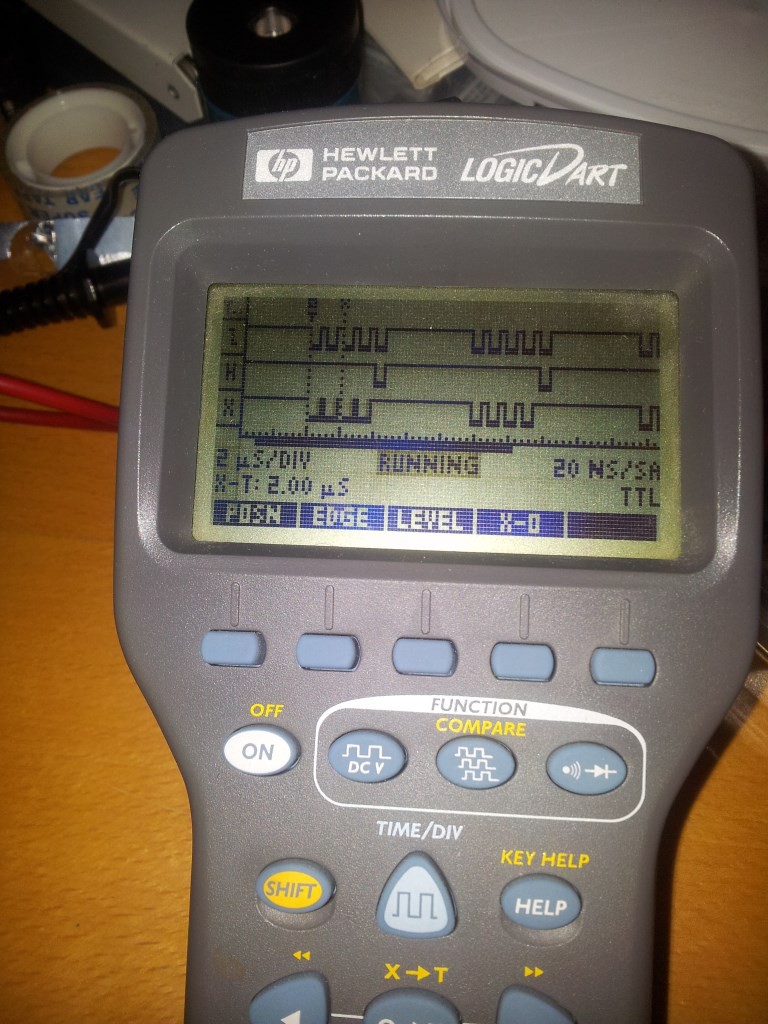
I did some further experiments trying to read data straight off the bus using an Arduino and the A23 line as an interrupt trigger on the Arduino to latch. As well as trying to rig up some DTACK circuitry to make that more stable at triggering, I never quite succeeded as the Arduino was never quite triggering when I wanted it so I couldn't tell if the numbers that I sometimes got were the ones I was expecting or random noise.
At this point I'm tempted to re-wire the circuit, make a better halt/reset circuit with debounce so that I'm certain that it's reset correctly. Another idea may to be make a single step circuit to allow for easier debugging as I only have a 3 channel logic probe at the moment.
Discussions
Become a Hackaday.io Member
Create an account to leave a comment. Already have an account? Log In.