 Hayden Kroepfl
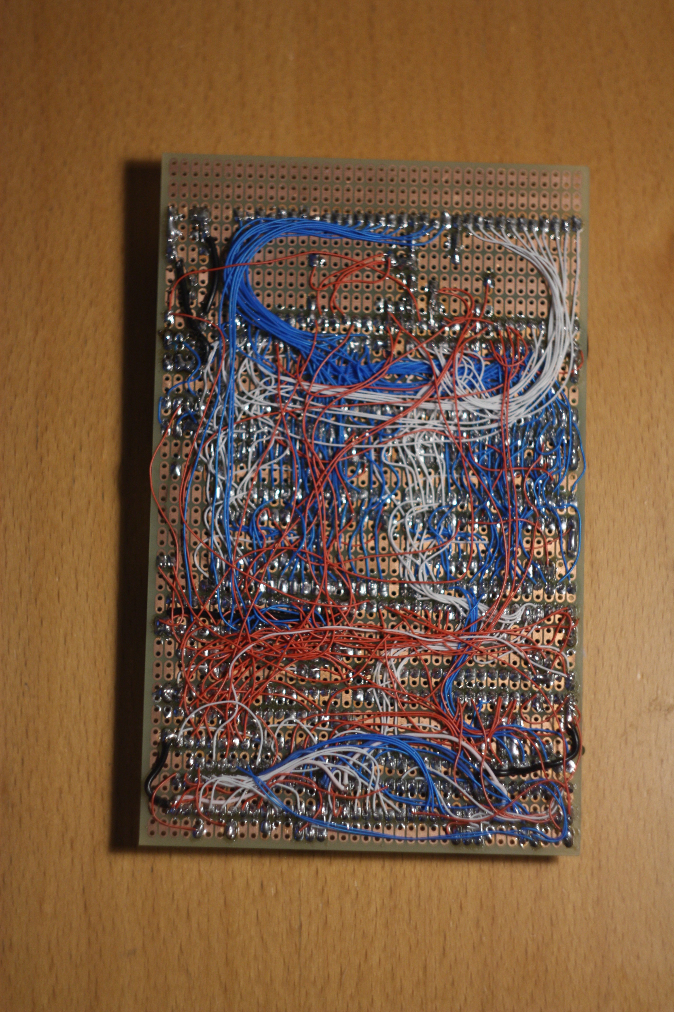
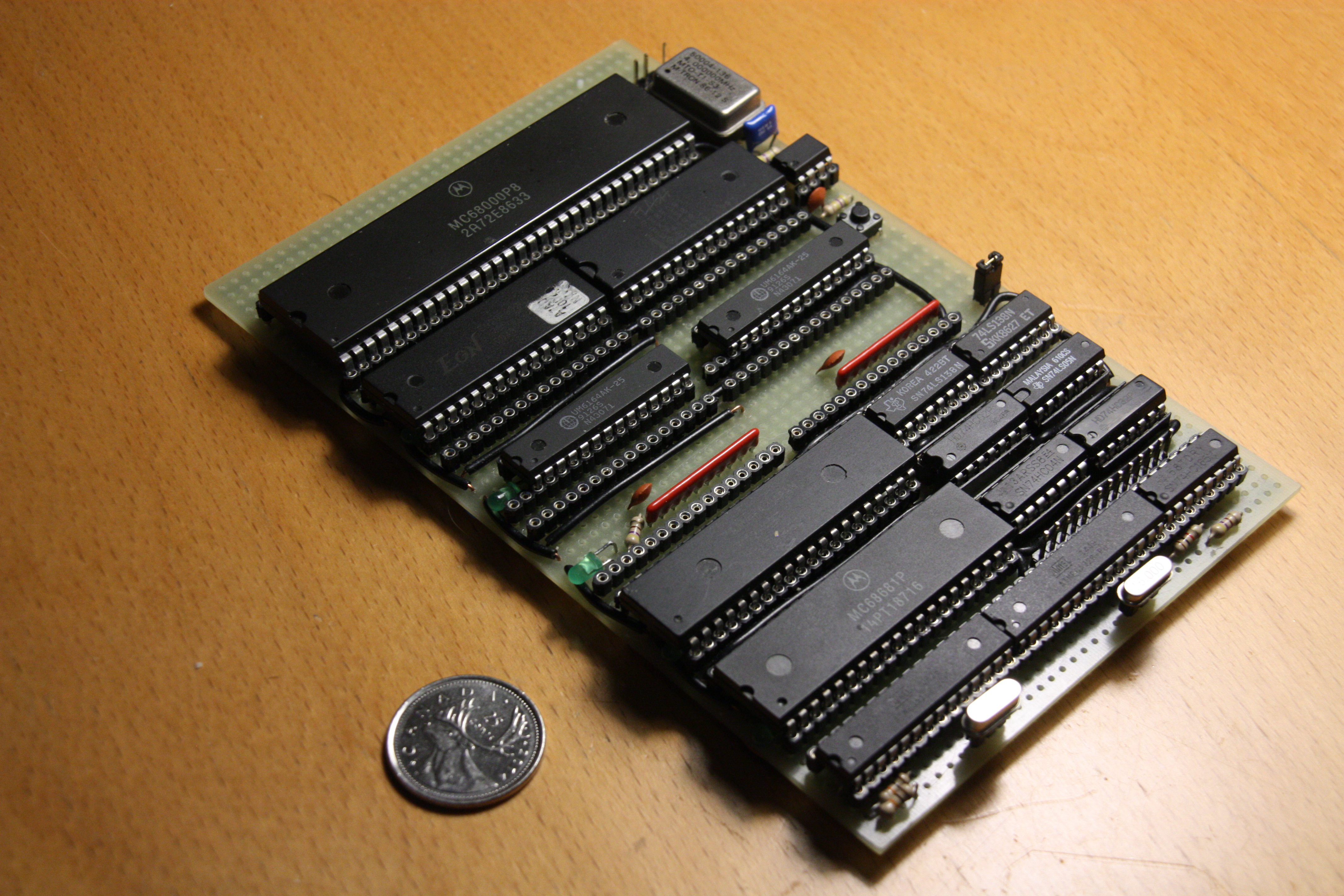 Well the breadboard part of my computer is no longer there. It's been all moved onto a single 3U euro-card sized protoboard. So I guess now I've got to change the title of the project. Was quite a bit of work to wire up the hundreds of point to point connections. All of it was done using 30AWG wire wrap wire, soldered point to point.
I changed a few things with the circuit when I moved it over. The main change is in how the address bus is decoded. I opted to go a bit excessive and used two 74138s to fully decode the entire 16MB space. Each output corresponds to a 1MB section of address space. ROM and peripherals are mapped into the lower 8MB, and RAM is mapped in the upper. On the board you can see two unused sockets, with the upper one having a RAM chip connected to part of it. The board is designed to take 2MB of memory in the form of 4 AS6C4008 4Mbit SRAMs, I just haven't ordered them yet. So for compatibility I added a inner header on the first RAM socket, so that I could put my 6164 SRAM chips in in the mean time.
One thing I should have done was to eliminate the 7404 hex inverter since I'm only using one gate of it, and I've got two NOR gates still unused.
Also added/changed was the video interface. I chose to replace my 32x24 column color text display with Grant Searle's 80x25 B/W display for AVRs. Along with the corresponding PS/2 keyboard and serial driver interface. On the board this can be seen at the very bottom with an ATMEGA168 on the left handling PS/2 and serial, an ATMEGA328 in the middle generating the video, and a 74HC165 at the right shifting out the video bits. One thing I'm thinking of doing is changing the interface AVR to instead scan a keyboard matrix taken from a laptop. This would allow me to more easily find a keyboard that would fit in my goal of making this computer into a laptop.
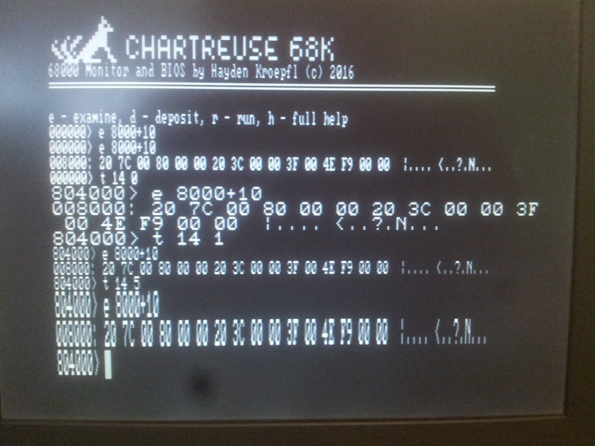
To go along with these changes I've updated the original monitor program on my GitHub to use the new memory map and display.
I've also partly re-wrote the monitor such that it can function as a BIOS for my operating system that I am currently written. I've added a number of BIOS routines accessible using trap #15 including standard screen writing, serial port access, a simple beep from the YM2149, and disk access routines. The new monitor/BIOS can also be found on my GitHub.
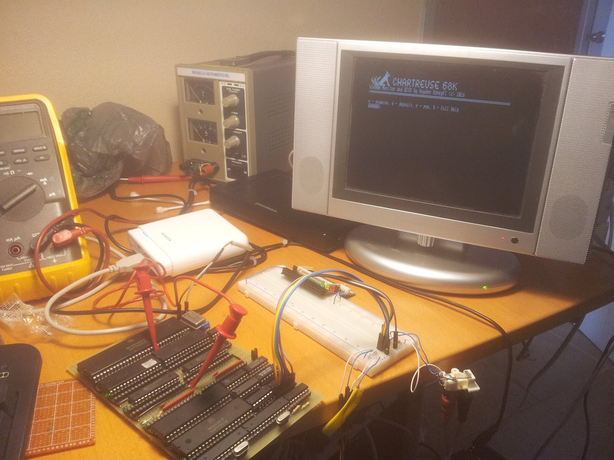
I still don't have any storage medium hooked up. I'd like to do IDE since it's trivially simple to implement with the 68k's BUS. Only requiring some logic to generate the positive level write and read signals from the R/W and AS pins. The problem though is that I've got almost no board space left. I've got just enough space to put an expansion header, or to put the IDE interface. What I really should have done was to put the video generator onto it's own board as it only requires 4 wires (Vcc, GND, Rx, Tx) to interface with the computer, while IDE would take something around 30.
There's also a slight hardware bug, due to one of my ROMs being a boot block ROM. One of the pins that's normally an unused or an address line pin is instead an active low chip disable. Since I wired the board such that I could replace my random pulled ROMs with new 4Mbit ROMs that pin was being pulled low by an address line. As a temporary fix till I get my ROMs in, I've bent the pin out of the socket. And used a clip to pull that pin to Vcc as unfortunately it can't just be left floating.
Discussions
Become a Hackaday.io Member
Create an account to leave a comment. Already have an account? Log In.