0%
0%
PCB 2012
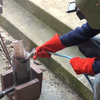
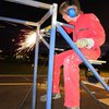
A few years back, I decided to revamp my engineering school's student PCB fabrication facilities.
 William Pauli-McCahon
Become a Hackaday.io member
Already have an account? Log in.
Just one more thing
To make the experience fit your profile, pick a username and tell us what interests you.
Pick an awesome username
hackaday.io/
Your profile's URL: hackaday.io/username. Max 25 alphanumeric characters.
Pick a few interests
Projects that share your interests
People that share your interests

 Carl Bugeja
 Elecrow
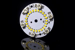
 SAYANTAN PAL
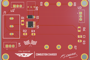
 aysenurkarga
Cool project, however, wouldn't it be better to do it the Stones way and paint it black? The inside of the box that is, to minimize non-aligned UV light bouncing off the walls and get cleaner lines?