 zaphod
I had always kind of assumed that it would be simplest to have the computer execute one instruction per clock cycle. it turns out this isn't the case. while my 1 instruction per clock, logic was correct I did not account for propagation delay.
here's a quick recap of how the computer's sequential logic fits together:

essentially the number coming out of the program counter is an address and is passed through the ROM access logic and selects and address (pink boxes). each address contains 8 bits of info (upper four are a value, lower four are a command). the value held in the ROM address indicated by the program counter is dumped onto the 8 bit bus. the upper half of the bus goes to the rest of the computer to do what ever the command tells it to. the lower half (the command) is sent through the instruction decoding logic, which is essentially a giant multiplexer (I.e 0110 (6 in decimal) goes in and 0000000001000000 comes out).
now if I wanted to load the upper half of the 8 bit ROM bus (V from now on), into the @ register I would need to pulse the load pin on the @ register. to do this I would program a value into the lower four bits of ROM (CMD from now on) that corresponded with the multiplexer output wire that was connected to the @ register load pin. I.e. if the 12th line coming out of the instruction decoding logic was connected to the @ register load pin I would set CMD equal to 1100. that way whenever CMD==12 the @ register is loaded with the value V.
there is a slight problem with the above explanation. V is asserted to the @ register input bus at the same time that CMD is fed into the instruction decoding logic, namely the rising edge of the clock. both values remain the same until the next rising clock, at which point they are replaced with the contents of the next ROM address. another thing to note: the @ register accepts a new value on the falling edge of the @ register load pulse. maybe you can see the problem. V and CMD change at exactly the same time. that means that the falling edge of CMD (the point at which the @ register loads) is the same point at which the value we are trying to load (V) changes, resulting iin garbage being loaded into the @ register.
solution? my first attempt at solving the problem was as follows. add an AND gate between the clock and the CMD lines and use the output to load the @ register. because the CMD and V values change on the rising edge of the clock but we need a falling edge to load the @ register we can use the falling edge of the clock to load the @ register. if the above paragraph made no sense fear not, here is the timing diagram:

load instr should say 'CMD'. basically Load @ = clk AND CMD. the above is logically correct, however you should note the word 'ideal' at the top of the page. as you may have heard propagation delay is a thing. I had assumed that this processor was small and slow enough that I wouldn't have to worry about propagation delay, not so! below is the 'real' timing diagram:
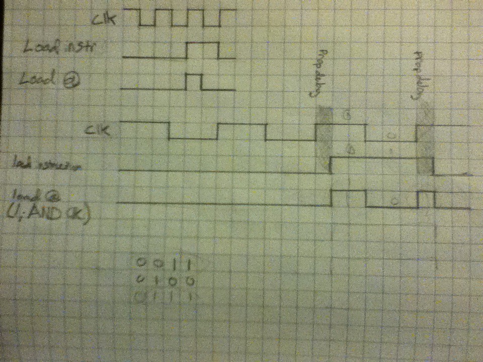
again, load instruction should be CMD. between the clock and CMD there are ~200 transitors. between clk and load @ register there are 2 transistors. there is a slight lag between the clk and CMD due to the number of transistors, compared to the AND gate between clk and CMD and load @. because of this the AND gate responds almost instantaneously and you get that little double blip on the @ register's load pin. this second blip also happens right as V is changing resulting in a garbage load of the @ register on the next clock. that stupid double blip took me two days to figure out.
I'm pretty sure that the double blip hypothesis is correct, it lines up with my observations quite nicely, however, I have not been able to observe this on my oscilloscope, although that's probably due to it being a pretty crappy oscilloscope and me not really understanding how to use it.
how does one solve a double blip? my best solution would be to split up the clock cycle. every other clock pulse would increment the program counter. the in between clock pulses would become a load clock that would be only be used to perform loads. I think I've got that circuit figured out, but I'll save that for another post.
if anyone has any ideas about how to catch the double blip with rudimentary tools, feel free to comment/message me. It would be nice to have direct confirmation before attempting to build some more logic.
***edit: I may have caught the double blip with my logic probe
Discussions
Become a Hackaday.io Member
Create an account to leave a comment. Already have an account? Log In.
[this comment has been deleted]
your idea of using both edges of the clock pulse is intriguing. I am hoping to avoid mucking around with the registers to much (they are already built and it would be nice not to have to rebuild them) however they could probably benefit from a redesign. I had also considered something like a debounce circuit, but I've since moved away from that because I'm worried about trying to do too much in one clock cycle, hence the idea of splitting up the clock cycle into a PC increment and a 'load clk'.
I would encourage you to post your project. I'm interested in seeing how other people go about designing processors, and the internet doesn't have nearly enough diy processors!
Are you sure? yes | no