zaphod
-
loops!
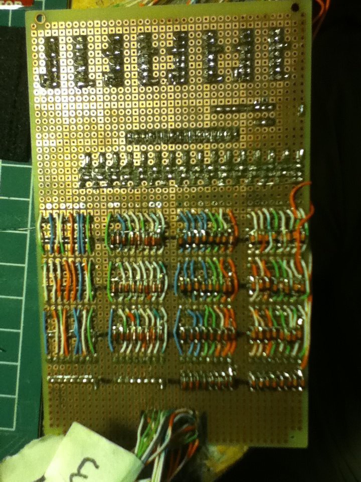
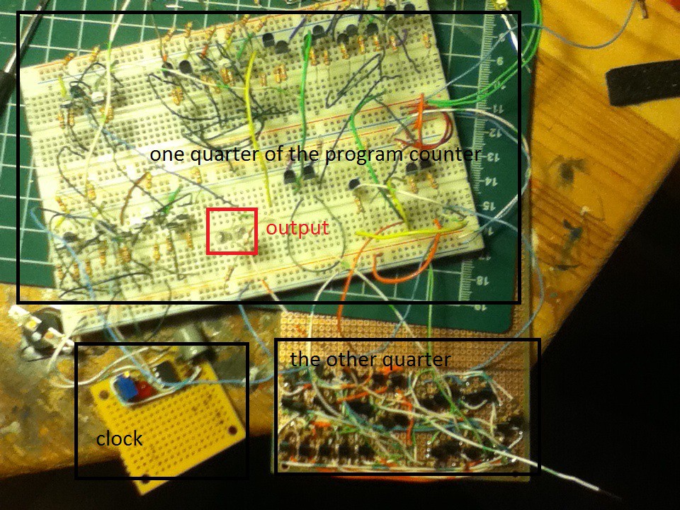
01/04/2015 at 17:04 • 0 commentsI finally cleaned my bench so I can now fit all of the computer on it at once:
![]()
it's not assembled yet, but that is basically a year and a half of work.
I'm working on getting it all put together but right now I'm testing functionality one piece at a time, which brings me back to the title. I was able to make to program counter perform a loop! essentially I executed a JMP command, by making the program counter jump to an address other than 'current address+1'. basically what I did was hard-wire in a jump to memory address 6 at memory address 7, so rather than counting like this: 0,1,2,3,4,5,6,7,8,9,10,11 ... it would count like this: 0,1,2,3,4,5,6,7,6,7,6,7,6,7,6,7 ... that lays the ground work for loops in software. another thing that I don't think I have mentioned is that the program counter reloads to 1+the value expressed on the input bus, I.e. if you wanted to go to address 6 you would enter 5, and when the PC reloads it would reload to 5+1. it works this way because the logic was easier to build, so when programming JMP commands you have to remember that if you want to jump to ROM address 'n' you must express n-1.
-
Almost Done (Maybe (But Probably Not))
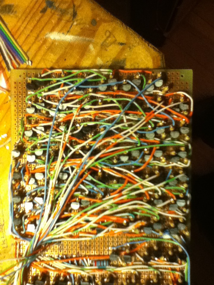
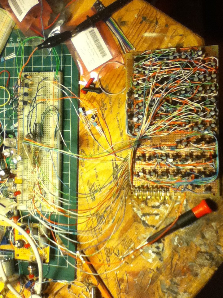
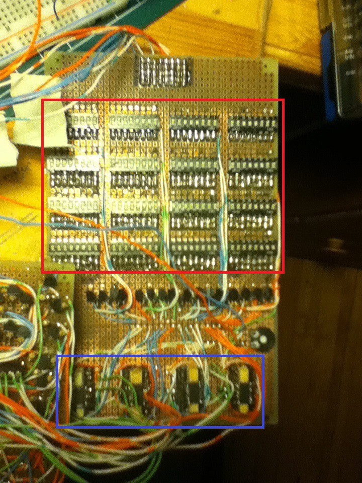
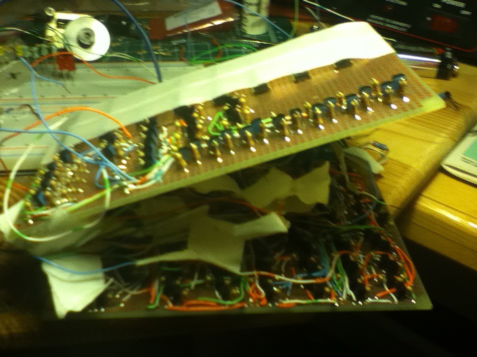
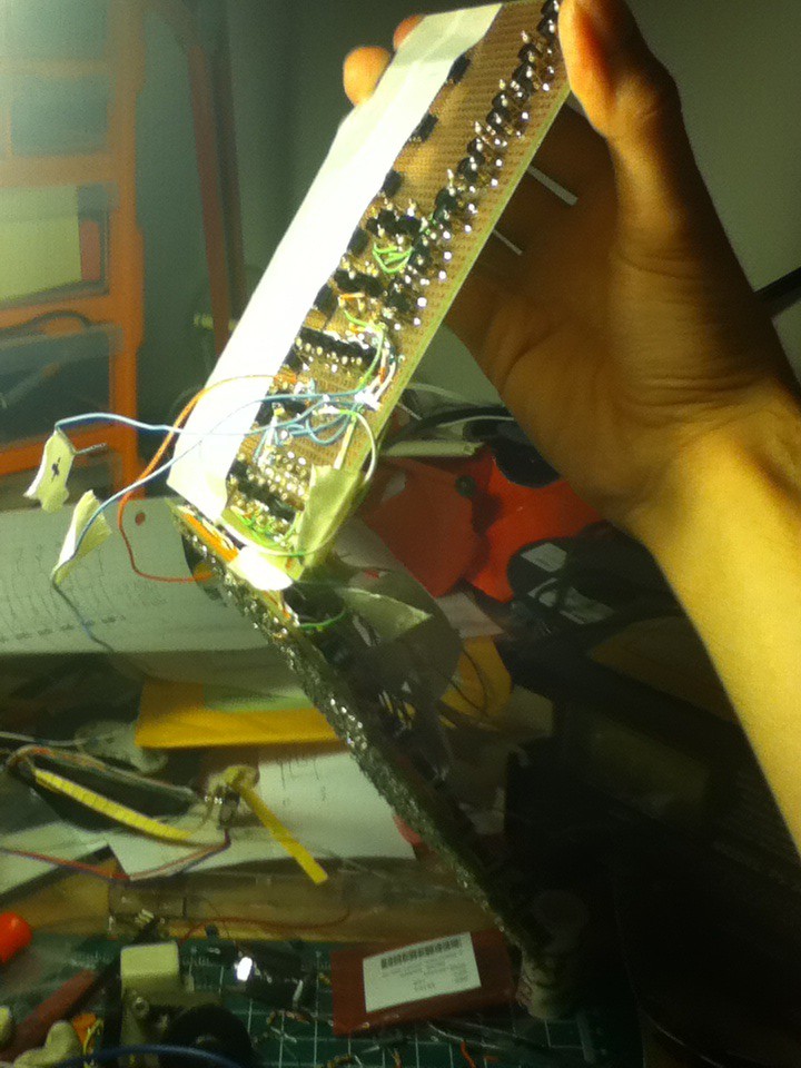
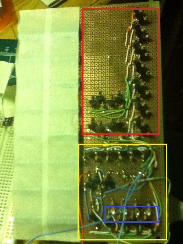
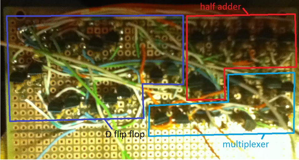
01/03/2015 at 22:35 • 0 commentsI finished the instruction decoding logic. here it is:
![]()
![]()
it's not quite done in these photos, but the finished version looks almost exactly the same.
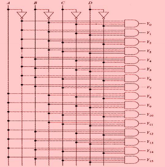
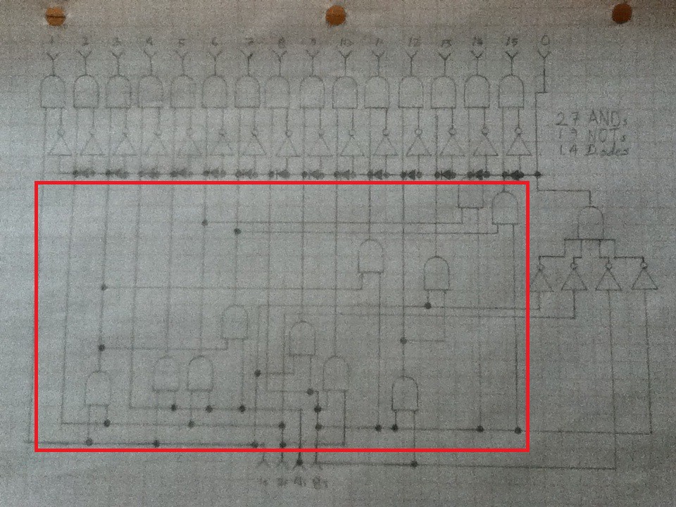
the instruction decoding logic's (IDL) job is to change a binary instruction into the appropriate control bits. I.e. if the next command is xxxx1000 (load @ register) I need to change that into a high on the load pin of the RAM. this means that the IDL is essentially a 1:16 multiplexer with the input held high. or this:
![]()
you may remember this circuit. I have already built one and it didn't work great, you can read about adventure here: (http://hackaday.io/project/665-4-bit-computer-built-from-discrete-transistors/log/7684-maker-faire-and-project-update)
basically the problem that I had previously was that I built the four input AND gates like this:
the above design reduces the number of transistors but ends up with sloppy logic levels. I ended up needing integrated circuits to fix this problem last time (see link above). this time I wanted to avoid ICs so I redesigned the four input and gates so that they now look like this:![]()
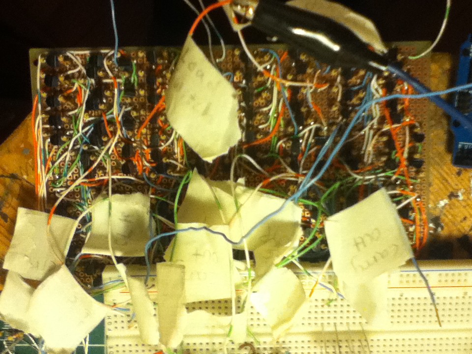
more transistors, but it works waaaaaaay better. astute observers will notice that the above design is just 3 two input AND gates. this method takes 50% more transistors but it is worth it in my opinion. after I had the AND gates built it was basically just a whole lot of boring wiring. and then I tested it and it didn't work uh-oh. the first thing I did was mess around with some resistor values on the inverters, and then it almost worked. after much hunting I determined that the input to one of the inverters was higher than it should be almost all the time, and seemed to be crossed with another input. it couldn't be a dead short between two pads on the board because the resistance between the inputs on the two inverters was extremely high. I figured it must be a solder flake bridging to pads, but after much inspection and cleaning the bug persisted. for reference here is the solder side of the board I'm working on:![]()
when I was laying out the board I drew some pencil lines on the top so that I would know where to build things and to make sure that each of the AND gates was the same size. it turns out graphite is conductive (kinda). yay! basically what happened was that a pencil line had bridged two pads, but since graphite has very high resistance my continuity tester did not see it as a short. after cleaning off the graphite everything worked as it should. moral of the story is: use some sort of non-conductive marking system to layout perfboard.![]()
whats next?
hypothetically the IDL is the last piece of logic to build. I should be able to connect all the pieces and have a working processor. however in real life it will probably be more complex than that. but that's the next step: start trying to get all the pieces playing together.
other stuff:
this project got an article written about it on hackaday.com. you can read the article here: http://hackaday.com/2014/11/22/a-4-bit-computer-from-discrete-transistors/
I imagine that's where most of you would have heard about this project, so thanks for all the views/skulls/follows.
-
multiplexers, multiplexers everywhere.
11/16/2014 at 16:31 • 0 commentsI finished construction on the 'reference multiplexer' here it is:
![]()
the image is inexplicably upside down (again)
Basically this takes in the the ROM data bus and switches it between the bank of LEDs and the rest of the computer. There is a tact switch that determines controls the address bit on the multiplexer. This multiplexer is necessary because it allows me to ensure that the ROM is outputting the correct values, without having it hooked up to the rest of the computer. The next piece to build is a 1:16 (de)multiplexer with the input held high. It will perform the functions of the control logic. This final multiplexer is supposedly the last piece of the computer left to build, so barring any major flaws in the sequential logic, the computer should be able to run a program.
-
the project continues
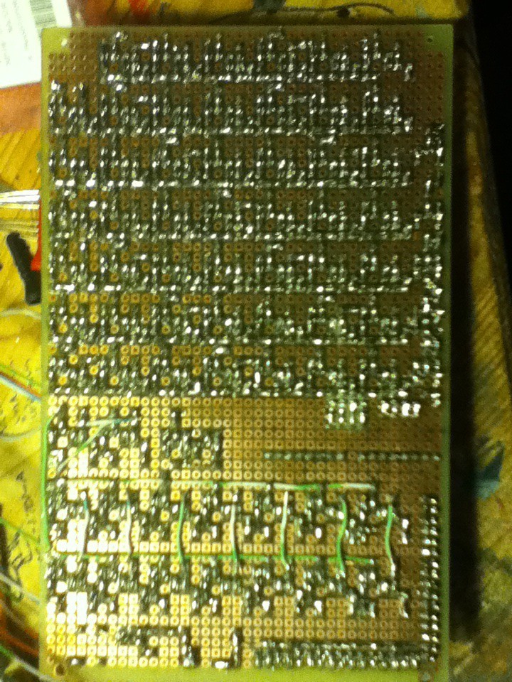
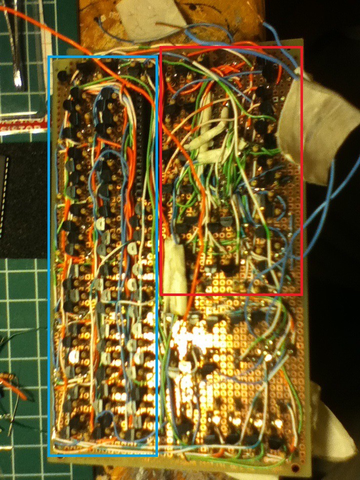
11/04/2014 at 02:55 • 0 commentsAs the title suggests this project is not actually dead in the water. My last update was just after the project was exhibited at Maker Faire, when I wrote that update the ROM was ~75% functional. Since then I have completed soldering the 128 diodes needed to bring the ROM up to functionality. The ROM board is now 100% complete, here's a couple of photos:
![]()
This is the top of the ROM board. The red box shows the actual physical memory. The ROM isn't some semi-abstract thing deep inside of the computer made up of magnetized spinning metal, but rather 128 individual toggle switches. The blue box shows where I ended up using LM339 comparators to clean up the ROM access logic. You can read about that wonderful series of mistakes here.
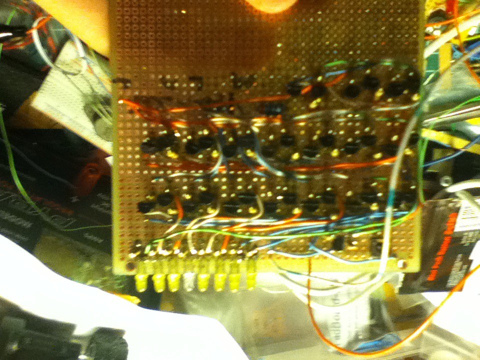
![]()
This picture shows the bottom of the completed ROM board on the left hand side of the image you can see the bus lines that feed into the switch banks, and if you look closely you can just make out the diodes I soldered on after the initial construction of the board. The completely new and unique series of mistakes that lead to the diodes can be read about in the link above. Anyway the mess of missteps that I made in the construction of the ROM is now over and the ROM works. To demo the completed ROM I connected the output of the program counter/multiplexer unit to the addressing lines of the ROM and the output bus of the ROM to 8 LEDs. I then toggled the following binary values into the memory:
00000001 // each line represents a memory address
00000010
00000100
00001000
00010000
00100000
01000000
10000000
10000000
01000000
00100000
00010000
00001000
00000100
00000010
00000001
When I hooked up a clock signal I effectively had a crude Larson scanner, which I made a .gif of but is too big to upload :(Now that I have a the ROM complete I'm ready to move onto the next stage of the project. the next piece to build is the instruction decoding logic. this will essentially be another 1:16 demultiplexer with it's input held high. The mux's address lines will be connected to the upper four bits (5-8) of the bus coming out of the ROM. the other four ROM lines will be a binary value to be operated on. however it isn't that easy. because I used comparators to clean up the ROM address signals I need another multiplexer. The comparator's reference voltage is set by a pot on the ROM board. Depending on various factors the pot need to be trimmed to ensure that multiple addresses aren't pushed to the data bus at the same time. The only way to ensure that two addresses aren't superimposed on top of each other is to probe the ROM's data out lines as you step through the code. If the data lines were connected directly to the next segment of the computer one could potentially effect the other logic farther down the line. the second multiplexer switches the ROM data bus from the instruction decode logic and onto a bank of LEDs so that I can trim the voltage reference pot.
TL;DR things are never as simple as they seem
The next things to build are the above mentioned 'reference multiplexer' (which I have started construction on) and the instruction decoding logic. these aren't terribly complex pieces of logic to build so they should be done soonish (maybe). Once the instruction decode logic is built the computer should (maybe) be able to run a program (provided every thing works perfectly). There is more I have to say but this post has gone on long enough.
-
Maker Faire and project update
08/19/2014 at 17:16 • 0 commentsa lot has happened since the last real project update, for starters I took this project to Maker Faire, photo:
![]()
I had a great time at Maker Faire and got to have a lot of interesting conversations with a lot of interesting people.
now, on to the interesting stuff.
in my last project log that actually discussed the construction of the computer I mentioned that I was attempting to build ROM access logic in the form of a 1:16 demultiplexer, as you may recall I was attempting to use this design:
![]()
(the red box shows how much I built)
I didn't have enough prototyping space to test the entire multiplexer, but the preliminary tests seemed to indicate that it would work, so I went ahead and built what is shown in the red box above. once it was built I started to realize that it had some pretty serious problems, first off due to the low gate fan out of RTL I wasn't getting usable signals out, in addition it turns out that the chain of diodes quickly degraded all signals passing through, even when I used diodes with low forward resistance. eventually I decided to abandon this design and take a look at how real multiplexers are built. my research came up with this design:
![]()
this design has much lower gate fan out and a much more predictable pattern. once again was unable to do a full scale test due to limited prototyping area, but the small scale results looked good so I went ahead and built it:
![]()
the red box show my (now abandoned) first attempt at the multiplexer, the second blue box shows the newer multiplexer design. the new multiplexer design seemed to work much better. the way that I tested the circuit was to connect the 16 outputs to 16 LEDs and then step through each address, this seemed to work and it appeared that only one LED light up at a time, just like in my small scale test. all good. I then proceeded to test the outputs with my first prototypes of ROM logic. this is where things started to fall apart. lines that had appeared to be off when attached to LEDs during testing where no seemingly on when connected too the next stage of logic. for a while I couldn't figure out what was going on, the LEDs seem to usally respond similarly to logic gates so I figured that the LEDs would be a good indication of what lines where on and which where off. I started probing around the circuit and found that some of the LEDs that were 'off' actually had enough voltage to be considered a logic 1 by the logic circuits I was connecting, but not enough voltage light up brightly. ideally I would have seen the dimly lit LEDs in my small scale testing, but as it turns out my desk lamp was bright enough that it overpowered the dimly light LEDs in both the small scale and large scale tests making it appear as though the circuit were functioning, when in fact it was not. because of this I didn't think to test the signals coming out of the multiplexer. the reason that I was getting a voltage in between my logic levels has to do with the construction of the four input AND gates used in the multiplexer. each AND gate consists of four transistors. the first has it's collector tied to VCC and the next has it's collector tied to the emitter of the first, and so on, until the emitter of the last transistor becomes the output, with the bases of the four transistors acting as inputs, the problem arises when the first three inputs are a one an the last one is a zero. the base-emitter currents of the bottom three transistors add up to produce a signal that is to high to be a zero and to low to be a one, hence the messy in between logic. at this point in the project I did not want to rebuild the multiplexer yet again and so I elected try and fix the problem with some analog engineering. eventually I managed to figure out that the part I was looking for was a comparator. this would allow me to set a threshold voltage and then repair all of my logic signals. I did attempt to build a comparator out of discrete components, but was unsuccessful so I ended up using integrated circuits, (blasphemy!) specifically the LM339 comparator. this did fix the problem and allowed me to move onto the next stage, ROM.
my idea for the ROM was to use 16 dip switches, each one playing the part of one ROM address. to implement this I thought I could build it like so:
I though I could bridge all off the pins on one side of the dip switch and connected them to the appropriate line on the multiplexer (address zero to line zero on the MUX, address one to line one on the MUX, etc.) from there I could set any number of the switches and when that line from the multiplexer went high I would only get a signal from the switches whose contacts were closed. I could then do this for all 16 addresses and connect the each line out of the banks of switches to the corresponding line on a larger bus, I.E. MSB of address one gets connected to the MSB of the bus forming a circuit that looks like this:
![]()
(once again unable to rotate photo)
with this design if signal line 0 was high and switch 2 (of address one) was closed line 2 one the output bus would go high. when the clock pulsed and the address was incremented so that signal line 1 is now high and switch 5 (of address two ) was closed line five on the output would then go high. this design seemed to work on paper and the tests that I did also showed it working so I built it. during the testing of the prototype I only ever had one switch closed per address (as in the above explanation) and this seemed to work, it wasn't until I was playing around with the ROM board and trying to get it to display patterns that I noticed a problem. if address one has one switch closed and address two has that same switch and another switch closed you get the contents of both addresses output on the bus at the same time, like this:
![]()
the red bubbles show switches that are closed, the solid blue lines show where electricity is flowing, and the dotted yellow line shows how the unselected address's contents are being superimposed over the selected one's contents. this problem turns out to be fairly easy to fix. all you need to do is add a diode on every line coming out of every dip switch. while this is a simple solution it requires 128 diodes. which is were I am right now. soldering diodes on the back of the ROM board. photos:
![]()
this is the top of the ROM board. on the right half of the picture you can see the 16 dip switches that make up the ROM, and on the right you can see the four LM339 comparators I had to use to repair the signals coming out of the multiplexer. in between are pnp transistors that are necessary to make the output of the LM339s useful as they are open collector circuits.
![]()
this is the bottom of the ROM board. I'm about 3/4 done soldering diodes onto the bottom of the board.
next steps:
the next section I will have to build is the control logic. this will take the individual machine code instructions and translate them into control bits (mostly flipping read write bits on registers). the most efficient way to build the control logic would be to build a 1:16 demultiplexer, but you saw how that turned out the first time around. I haven't been able to come up with a better way to turn binary numbers into individual pulses, but I don't think I can build such a large demultiplexer without needing to use comparators again, which I'd rather not do. anyway if you have any ideas about how to change binary numbers ito individual pulses or how to build comparators out of discrete components they would be welcome in the comments.
-
Design flaw
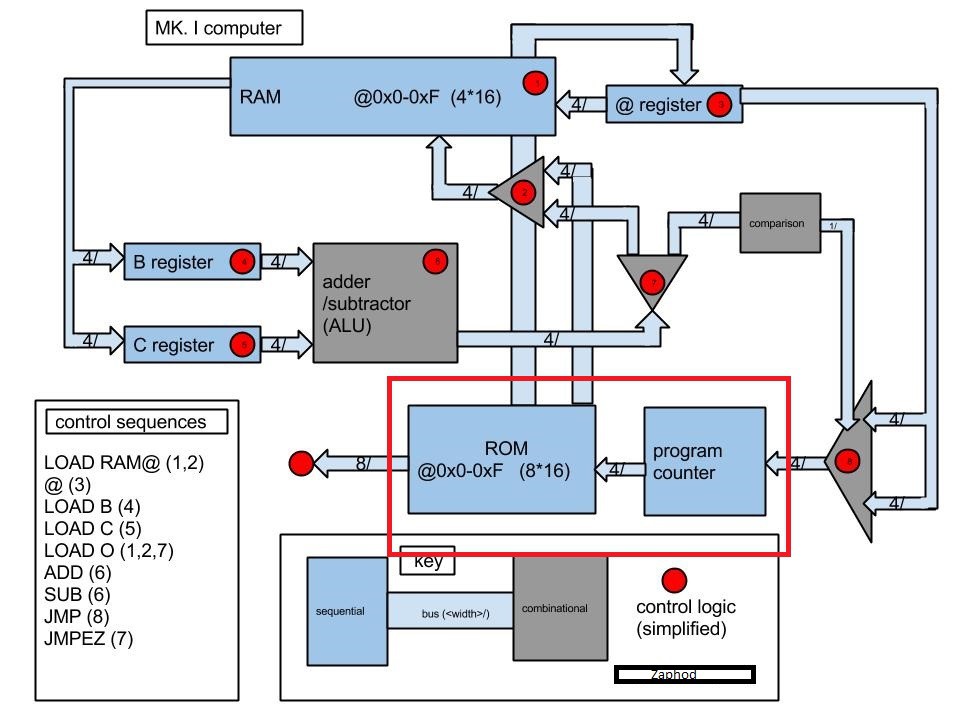
08/06/2014 at 00:56 • 0 commentsSince the processor is nearing completion I've been thinking about programming it. One of my ideas for a program was to have the user specify a binary value, and then have the processor fill every available ram location with that value. This program requires that the value held by the @ resister be dynamic, I.e. the value in the @ register has to come from ram. Now take a look at the block diagram; there is no provision for @ register values to come from ram. That's the problem. Here's my solution, stick a 2:1 4 bit multiplexer between the ram and the incoming values, one of the inputs would be connected to rom, the other input would be coming from ram. the added command: RAM @ would then flip the multiplexer's control bit and the @ register's load bit. Pictures and updated schematics are forthcoming.
-Zaphod out
EDIT:
I've been thinking. specifically I think i found a problem with my solution. imagine a value from RAM is loaded into the @ register. to do so various control bits need to be flipped: the read bit on the RAM, the multiplexer bit, and the load bit on the @ register. at the beginning of the clock cycle the @ register holds the RAM address where the next RAM address is stored, I.E. @=0000 (RAM location zero) RAM0=0110 (value stored in RAM location indicated by the @ register.) when the clock goes high RAM0 is moved to @ (@=0110). now the @ register is pointing at RAM6. all good so far. it goes wrong now because all the control bits are still flipped, so the processes happens again @ is set to RAM6. now it happens again, @ is set to the value in RAM6 and so on... infinitely until the clock goes low, a value stored in a RAM address is also it's address (I.E. RAM16=1111), or something breaks and the magic blue smoke is released. I could rectify this problem by adding a half-clock delay on all of the appropriate control lines, however that produces a lot of hairy combinational logic. I think a better solution would be to replace the RAM @ command with a MIGRATE command. this would move the value in one of the registers to the @ register, side stepping the combinational logic. this solution still requires that I build another mux.
-
state of the project
07/31/2014 at 17:18 • 0 commentsthis isn't a build log, just an update on the state of the project and an explanation of why there hasn't been any updates of late. first off, I will be exhibiting this project at maker faire Ottawa(!). so if you're in the national capital region for August 16th and 17th (2014) you should come out to the Science and Tech museum, link. I haven't had time to post any real updates because I have been busy trying to finish the computer, at this point it looks like it may be functional for maker faire, however that is still tentative. my goal is to display the computer (hopefully running a program) along with posters and potentially a couple of 'demo gates' that faire-goers can interact with.
TL;DR: come to maker faire Ottawa (August 16th&17th) to see the computer.
-Zaphod
-
program counter, multiplexer and memory
06/26/2014 at 16:30 • 0 commentsthis is what I've been working on:
![]()
![]()
(I was once again unable to flip the photo)
for reference here's what you're looking at:
![]()
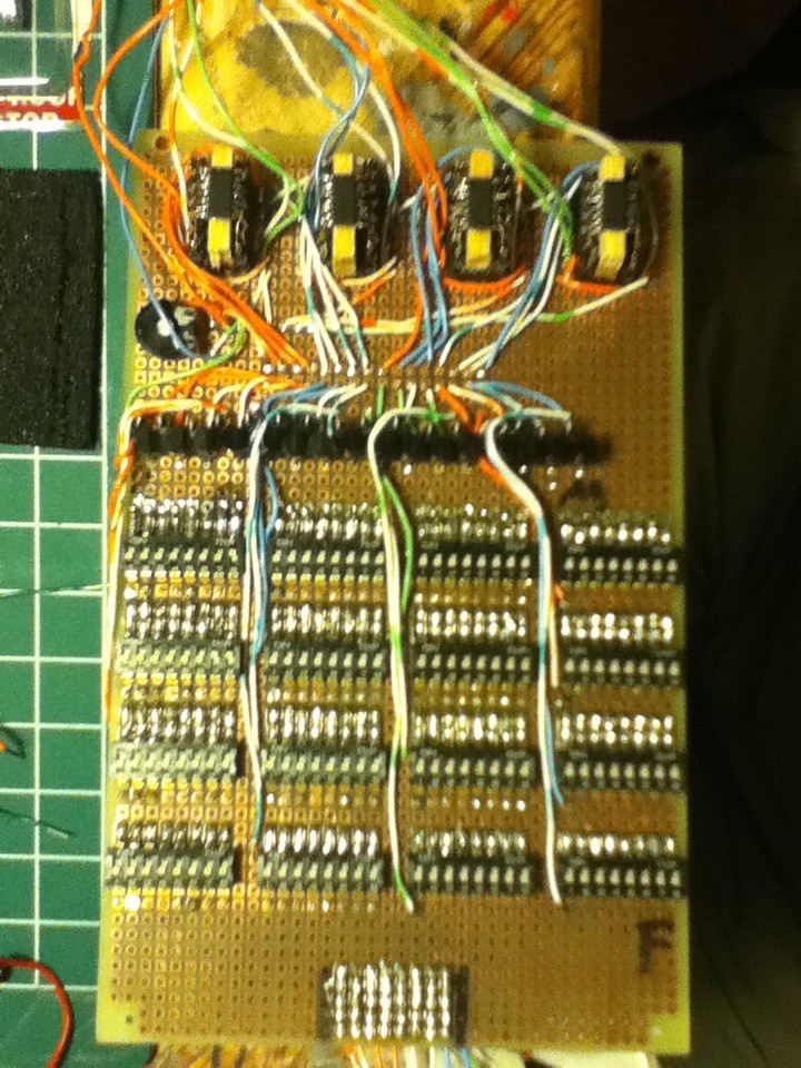
you may recognize the bottom board. it's most of the program counter. the top board is the extra logic that is necessary for the program counter, that I could not include on the bottom board. additionally the top board contains the beginnings of the ROM access logic. the stuff underneath the masking tape are the 16 DIP switches that will make up the ROM.
![]()
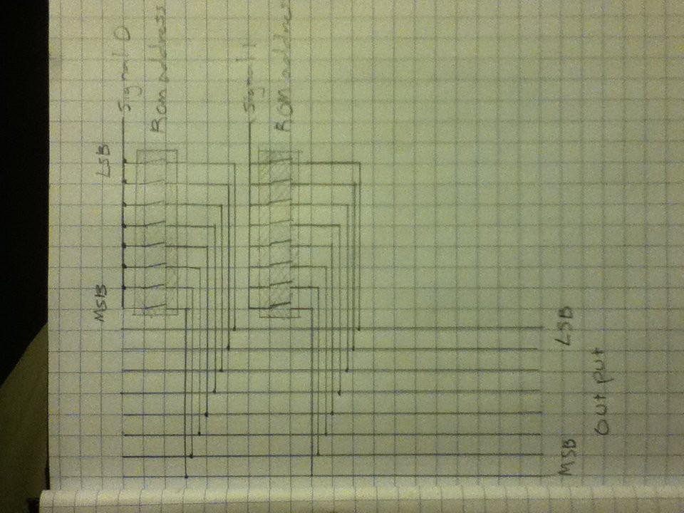
this is the top board. the stuff in the yellow box is the extra program counter logic. the blue box contains LEDs that will read out the memory address that the program counter is currently pointing to. the stuff in the red box is the beginnings of a multiplexer for memory access. this is the design I am using for the decoder half of the multiplexer:
![]()
the red boxes correspond. basically what this circuit will do is translate a 4 bit binary number, say 0110 (6) into a single pulse on a 16 bit line, e.x.:
0110 becomes:
0000010000000000
and 1001 becomes:
0000000010000000
etc...
basically this circuit will allow a 4 bit number to select one memory address. the reason that the program counter counts in binary (0000, 0001, 0010, 0011, 0100, 0101...) rather than like this:
0000000000000000
1000000000000000
0100000000000000
0010000000000000
0001000000000000
0000100000000000
etc...
is because the program needs to be able to reset the program counter to a new memory address, however the computer can only process four bit numbers, so if the memory addresses were 16 bits wide loops would be impossible.
the next step is to build the remaining memory access logic.
-
program counter pt. 3
05/24/2014 at 21:18 • 2 commentsI'm back!
last weekend I got around to soldering the ~120 transistors that make up most of the program counter.
![]()
as of right now I think this is the most densely packed board I have made for the computer (and possibly ever).
here's the schematic:
![]()
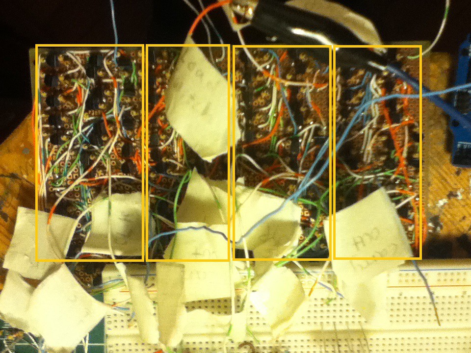
and here's how the board is divided up:
![]()
the yellow boxes in the photo correspond to the yellow box in the schematic.
some astute viewers may have noticed the AND gate and the inverter in the above schematic. these are not on the above board because I ran out of space, hence the breadboard in the below picture:
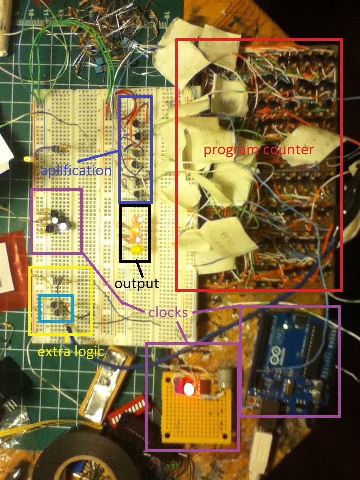
![]()
the red is the majority of the logic for the program counter. the yellow box denotes the extra logic. the blue box within the yellow box is the missing AND gate, the other transistor is the NOT gate.
the black box is the output. the output is a four bit binary count:
0000
0001
0010
0011
0100
etc...
it is currently represented by LEDs but will eventually be fed into the ROM as an address value.
the dark blue box is some amplification. each section of the program counter is essentially a half-adder, so the way that each section effects the next section is by sending a 'carry' bit to the next half-adder down the chain. it turns out that when I implemented this the carry bit was too weak to be read as a 1 by the next section of the circuit. because of this it is necessary to amplify each of the 'carry out' lines all the way down the chain.
the final boxes are clocks. the presence of three boxes marked 'clock' begs the question, why are there three clk sources? the answer is that I've had some trouble finding a good source. the first potential source is the Arduino.
pros of the Arduino as a clock:
-I can accurately say the processor has a clock speed of 'X'
-I can easily change the clock speed, to try to find the fastest speed that the processor will run at.
cons:
-it's an entire Arduino (!!!)
so I will probably not use the Arduino as a clock source, because it is overkill. I could potentially integrate the clock output onto the ATmega that is acting as RAM, however, this would probably cause more timing problems than it would solve.
the second second potential clock source is the 555 timer in astable mode.
pros of the 555 timer:
-easy to change clock speed
-simple
cons:
-I can't find the exact clock speed without some math, and even then it's debatable as it relies on component tolerances, and the various parasitic forces at play within the circuit
-it's still a chip, and this is a discrete transistor computer.
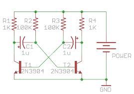
the third potential clock source is this circuit:
![]()
i'm not sure what it's called but it does seem to generate an oscillating waveform.
pros:
-made out of discrete components (yay)
cons:
-I can't calculate clock speed, (it requires math that I don't yet know how to do)
-it doesn't seem to play nice with my program counter. I have no idea why this circuit doesn't work with what I have built. my hypothesis is that the square(ish) wave that it outputs is too noisy, and is causing some kind of incorrect count. this is just a hypothesis, and to test it I would need an oscilloscope, which I don't have access to.
as of now I don't have any idea of which clock I will use, however right now I would give the edge to the 555 timer. if you have any suggestions, about discrete transistor oscillators, or why the above circuit doesn't work feel free to comment.
-
program counter pt. 2
04/14/2014 at 21:54 • 0 commentsI successfully built a quarter of the program counter on perfboard. the bread boarded one and the perfboarded one have been connected and I have a (partially breadboarded) 2-bit program counter, it counts from 0 to 3 and then rolls over to zero again, and can be reloaded with any new address.
![]()
for reference the above circuit is 15 perfboard holes tall (1.5 inches)
![]()
the above picture is of a completed 2-bit program counter (half of what I will eventually build entirely on the perfboard)
underneath the words 'program counter' over the bread board is some additional logic, specifically an inverter and an AND gate, this is for the reload logic.
4 bit computer built from discrete transistors
This project is an attempt to teach myself about the inner workings of computers. Naturally I started from the bottom up.