 matseng
Log Entries
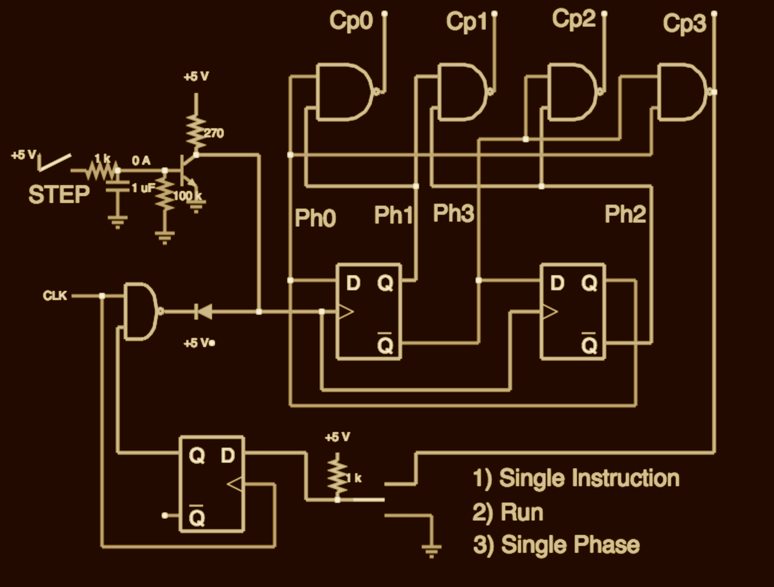
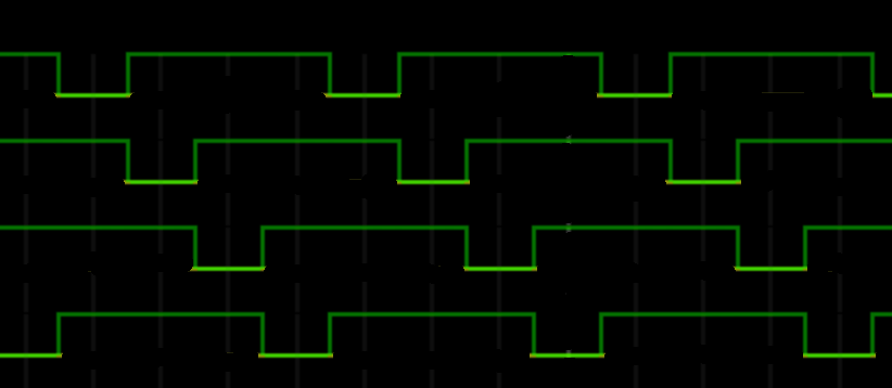
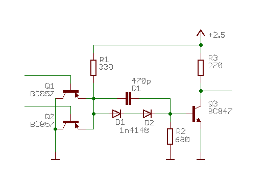
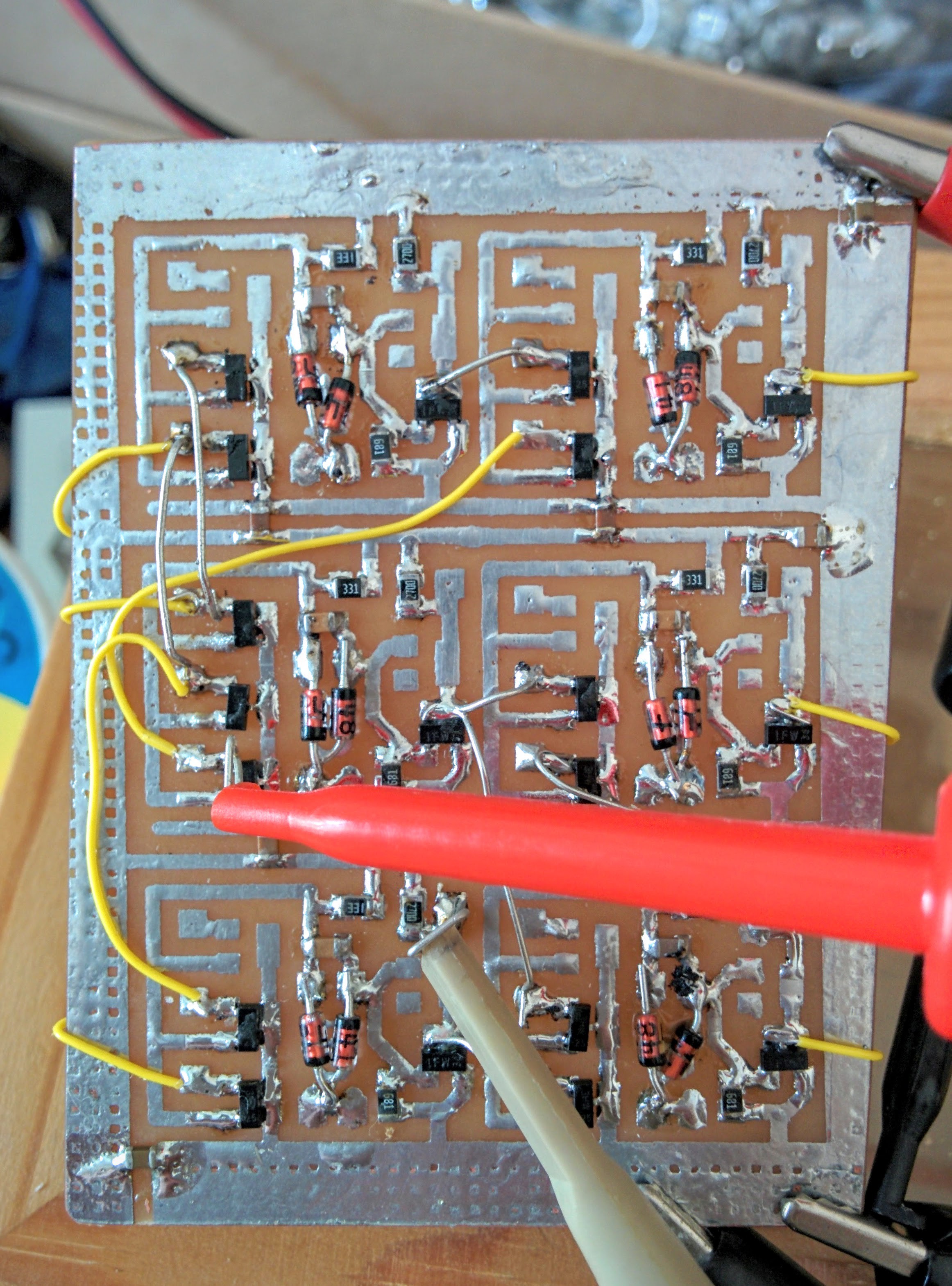
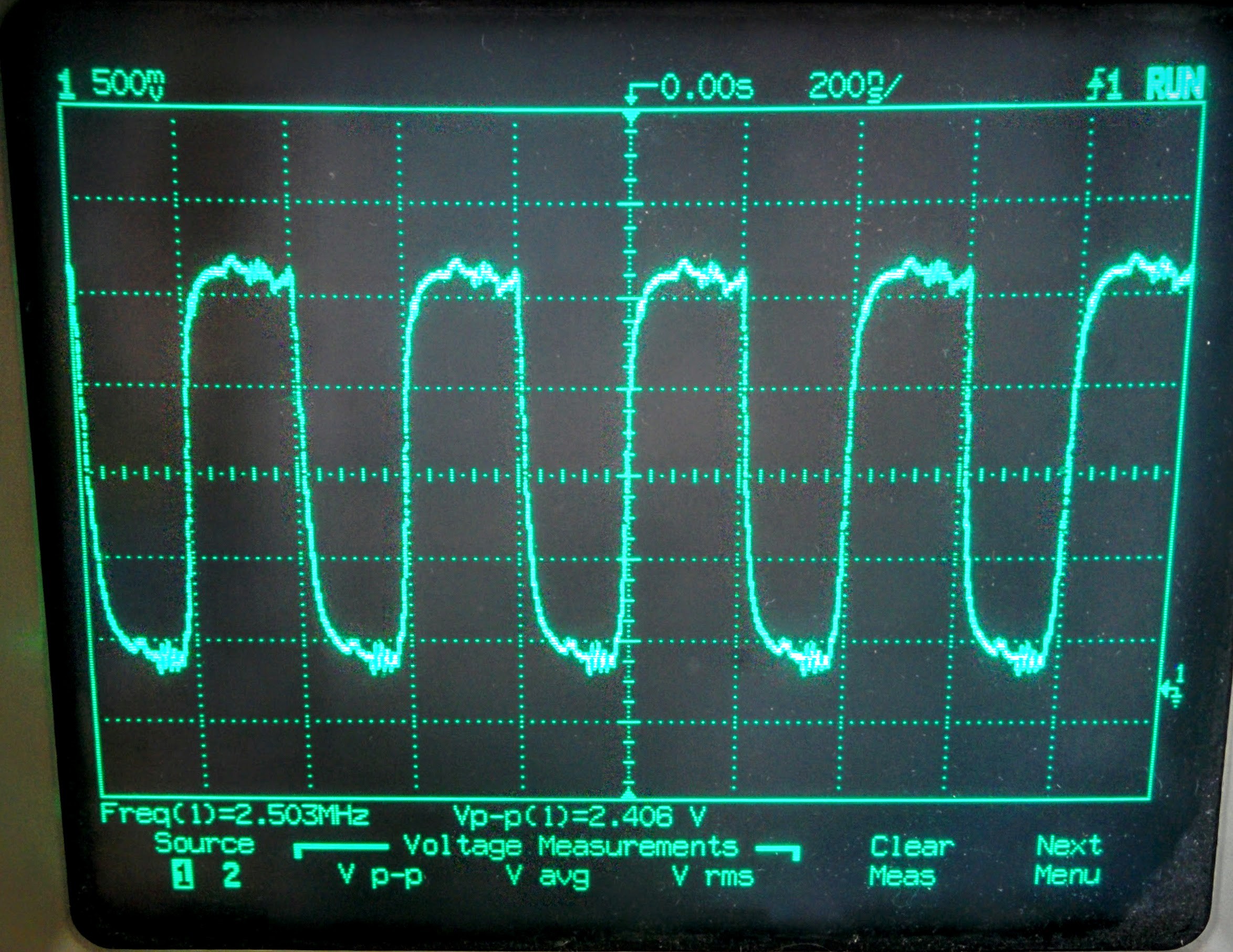
- Four phase clock generator
- More speeeeed!
- Testing speed of D Flip Flops
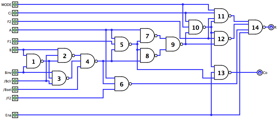
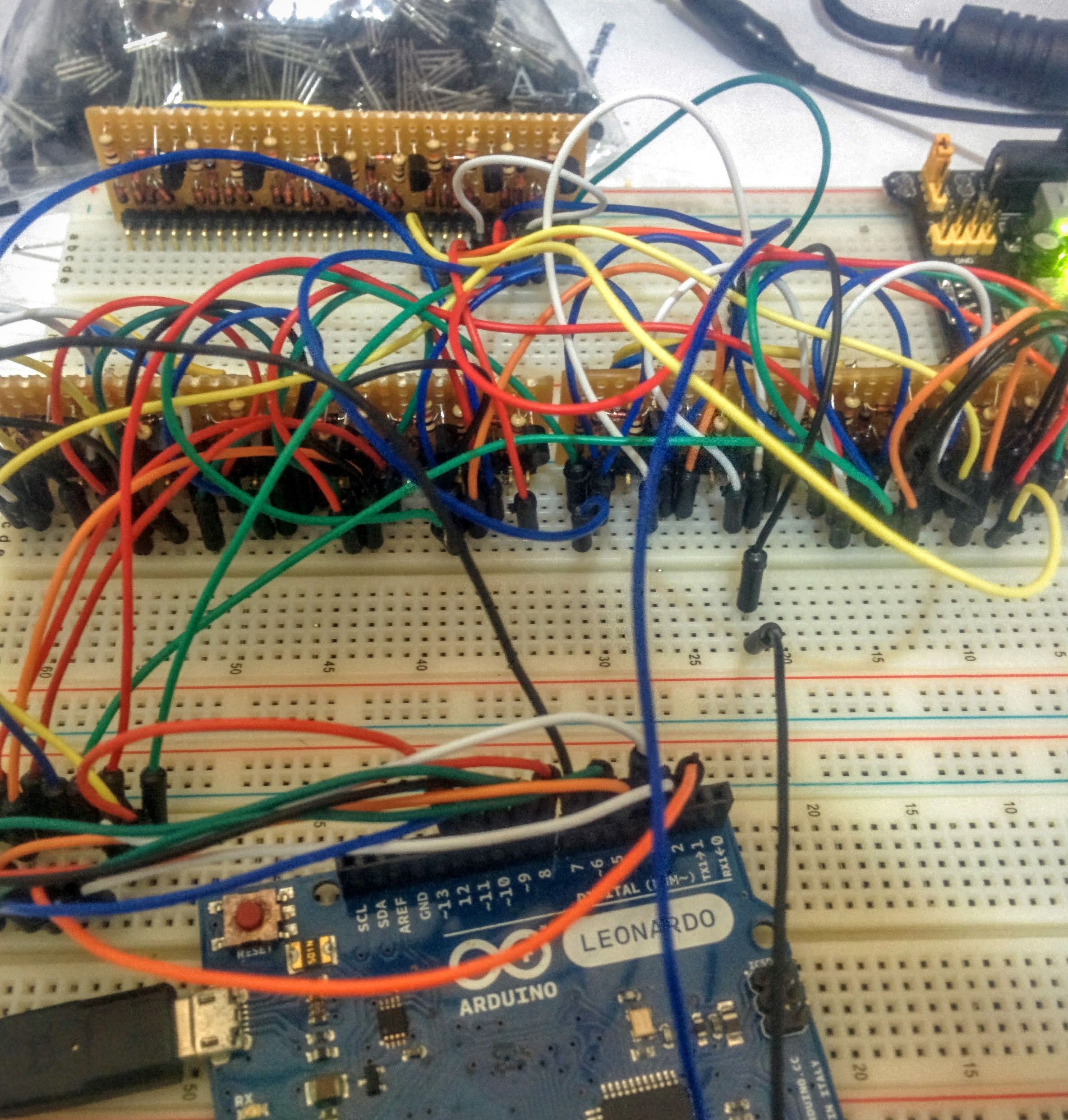
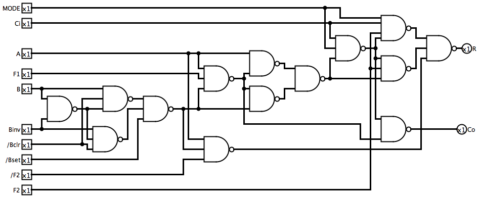
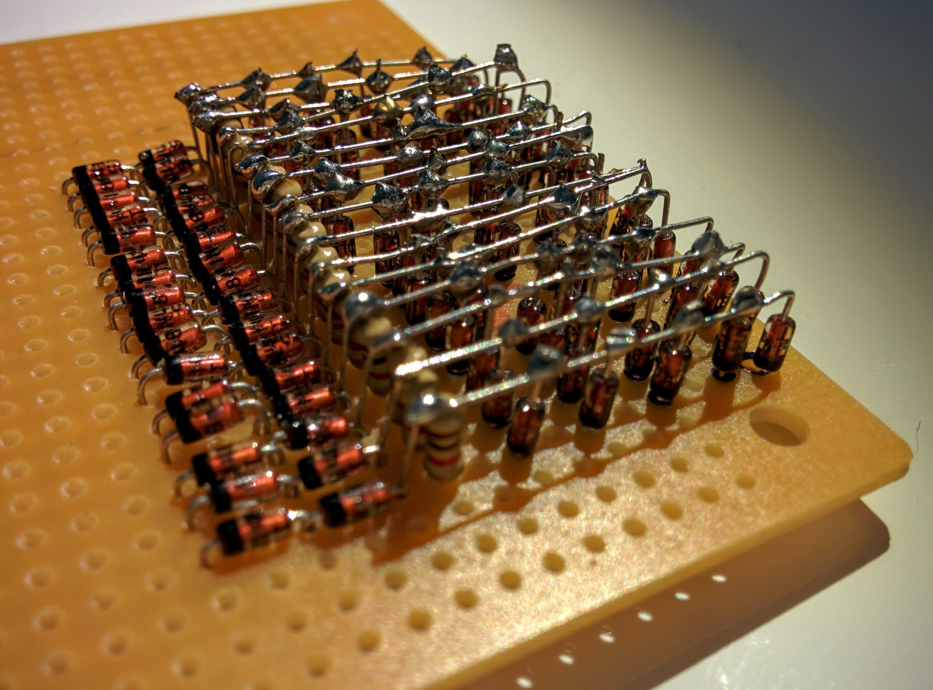
- One ALU Slice tested with real hardware
- ALU Slice design done
- Feeling the pressure
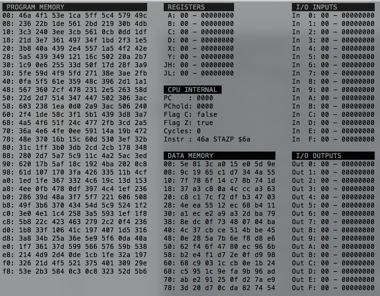
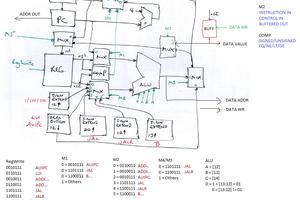
- CPU Emulator
- A 4-to-16 Decoder board
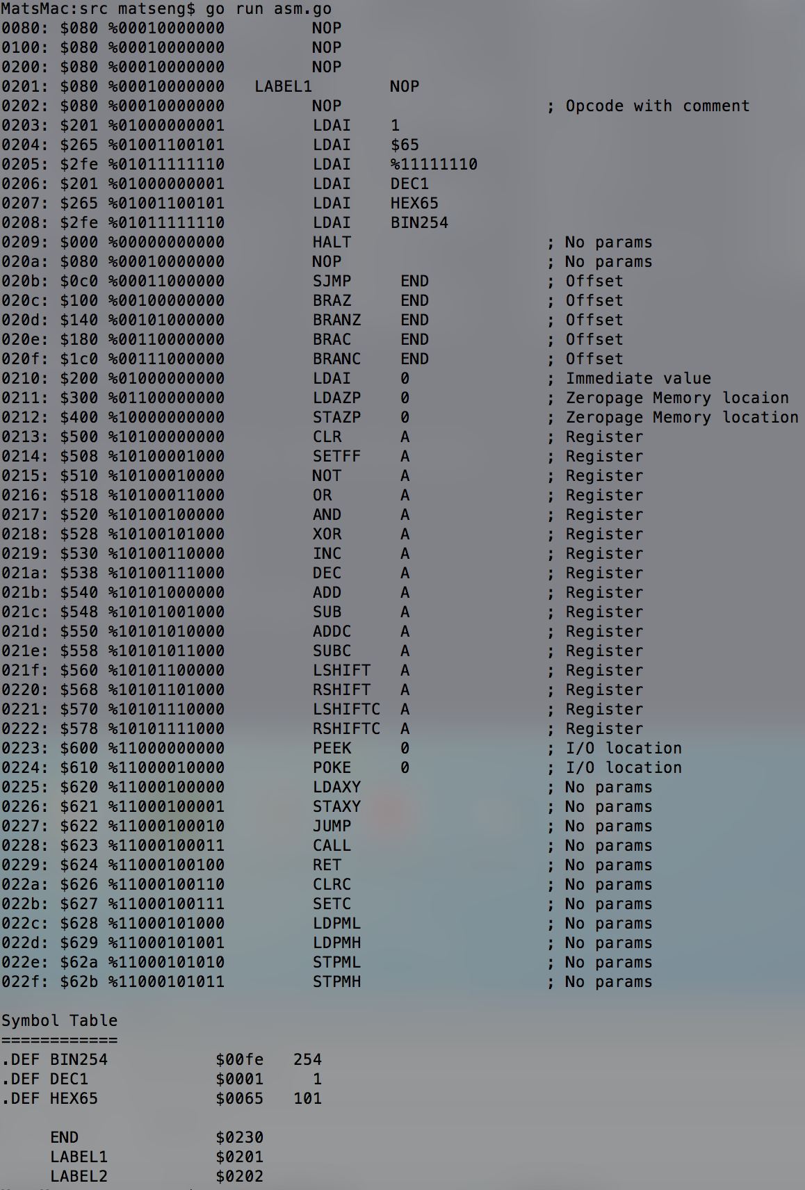
- Assembler for this CPU
- Instruction set
- UART RX Timing board done
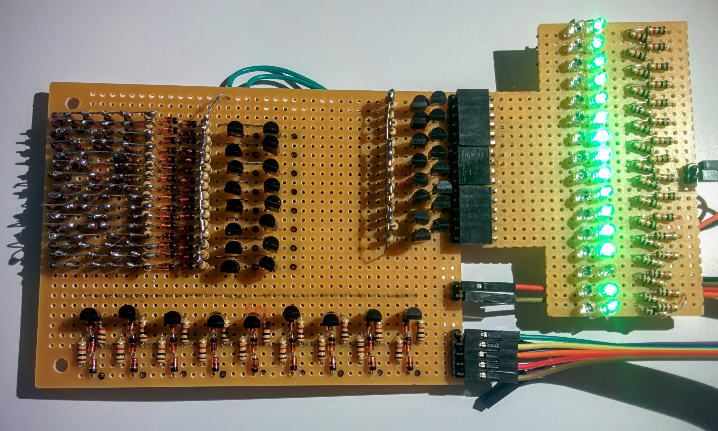
- Bus Viewer with LEDs
- Testing of comparator-chain
- Added glitch detector for RX
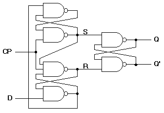
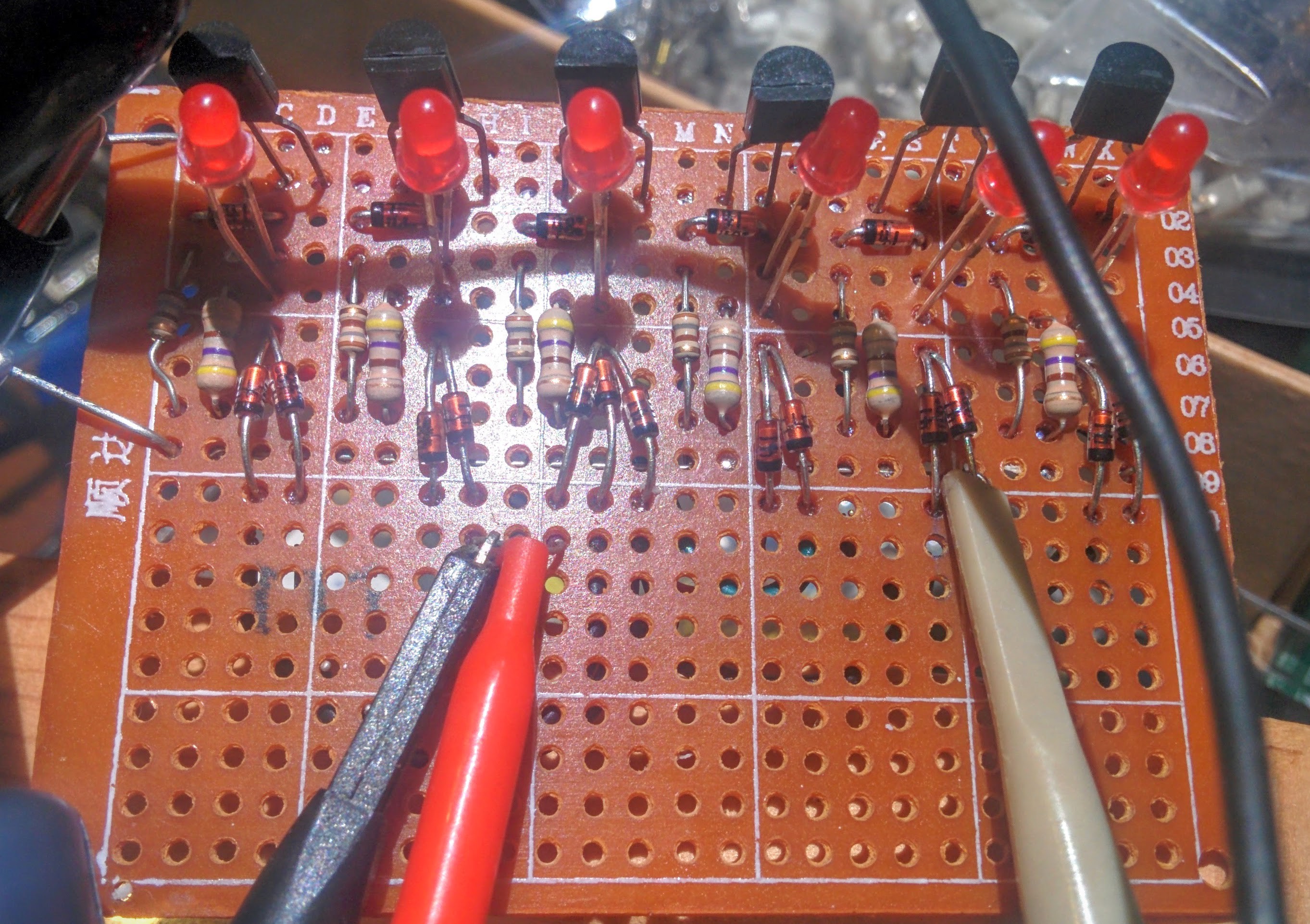
- Soldering of the octal D-latch
- Received some parts
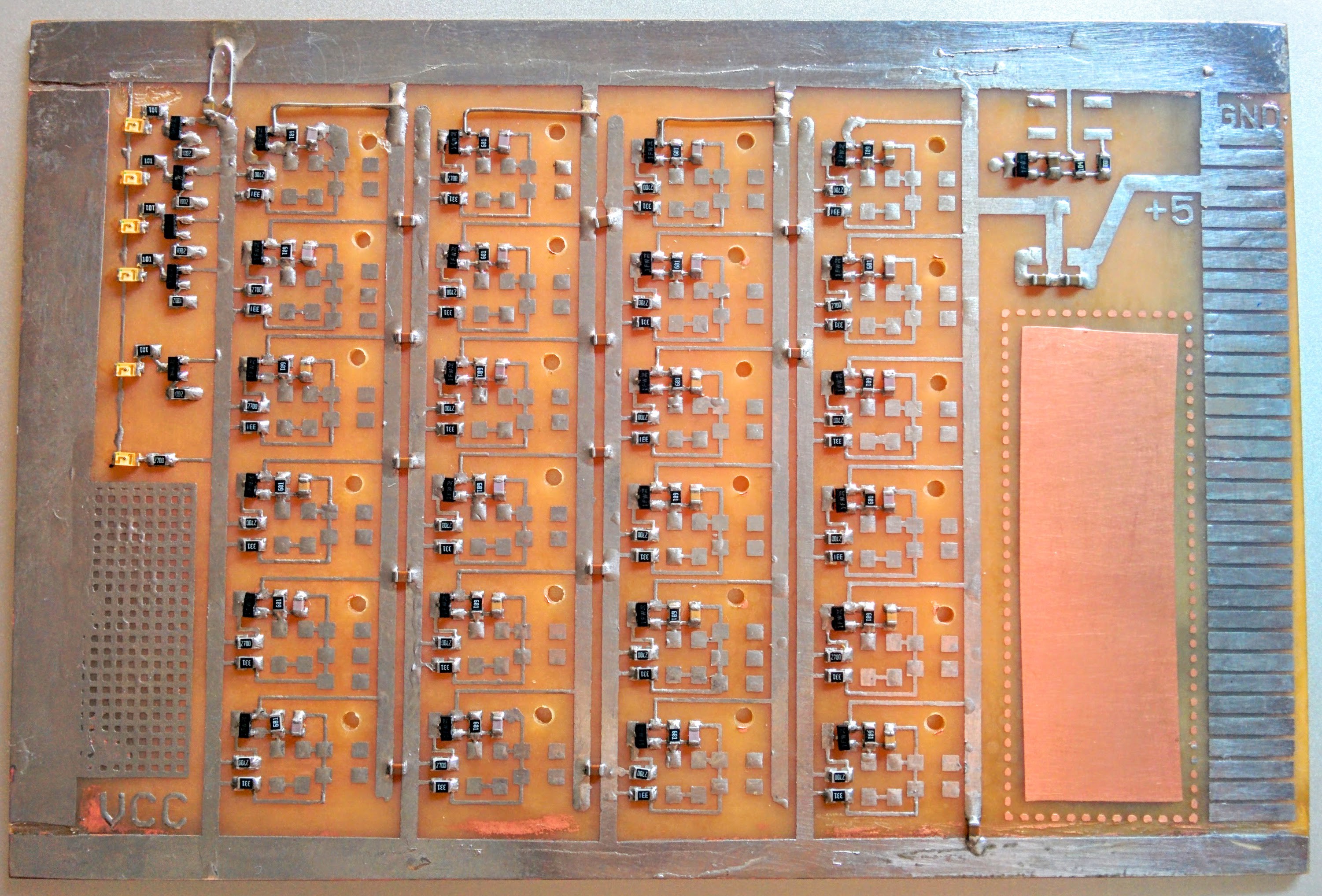
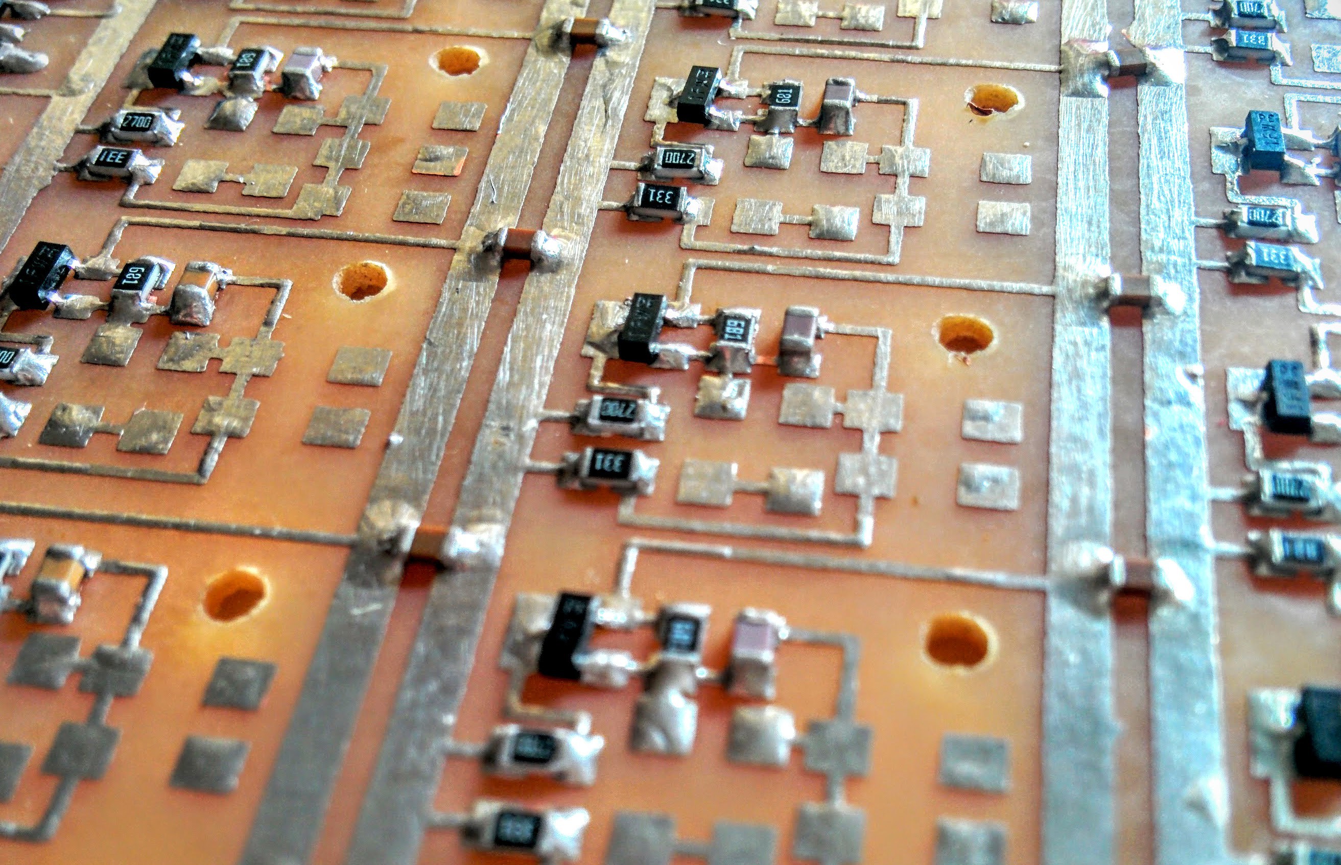
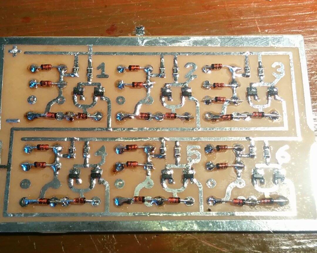
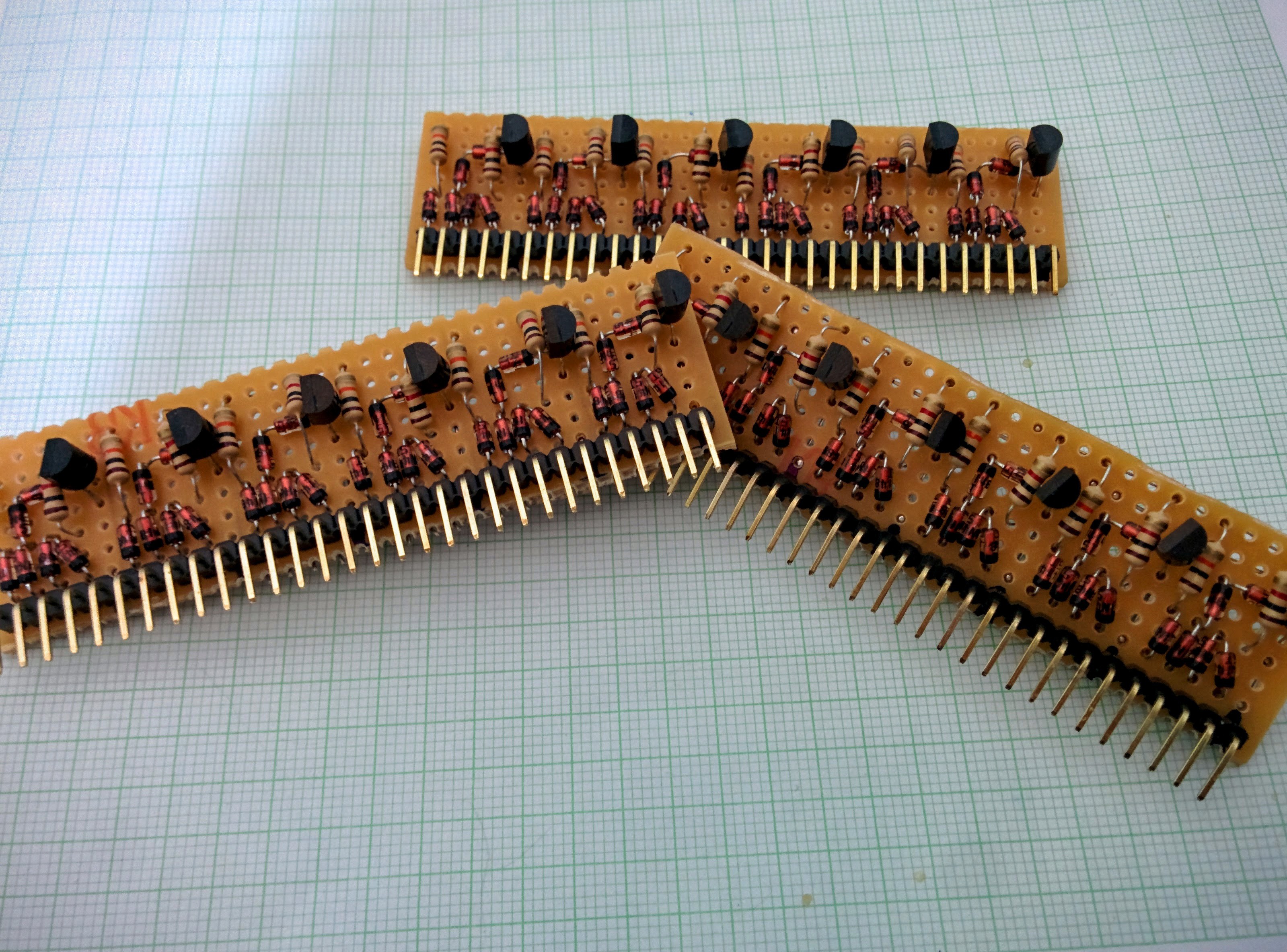
- Ordering NAND PCBs
- UART-RX


 Phil Wright
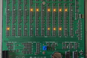
 Joe Wingbermuehle
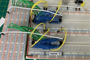
 Brandon Reinhart
 Dave Collins
after the apocalypse, we won't have internet tho. Next project: WiFi service and router from resistors and magnet wire. XD nice job, hope it's coming along one way or another