-
Project put on hold for a while
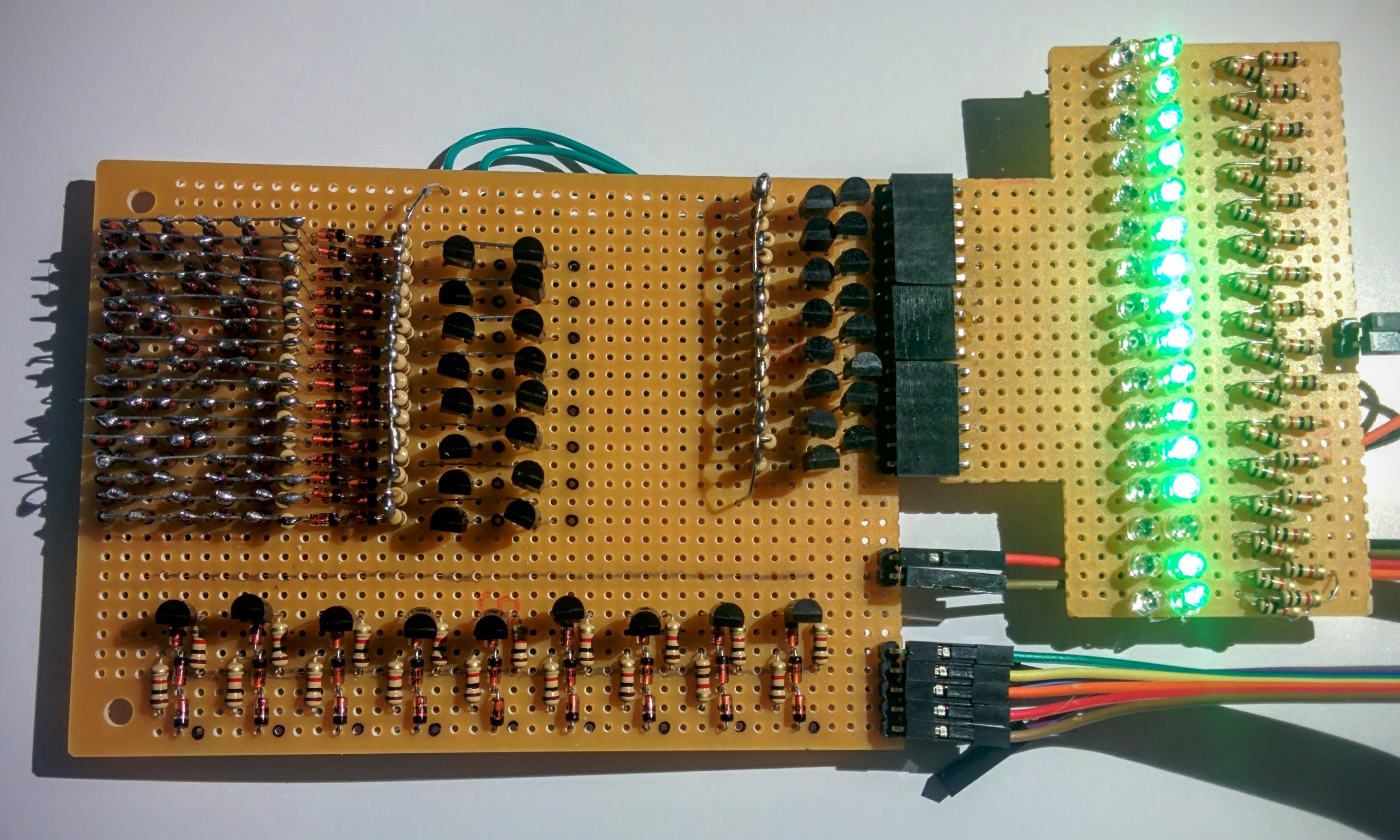
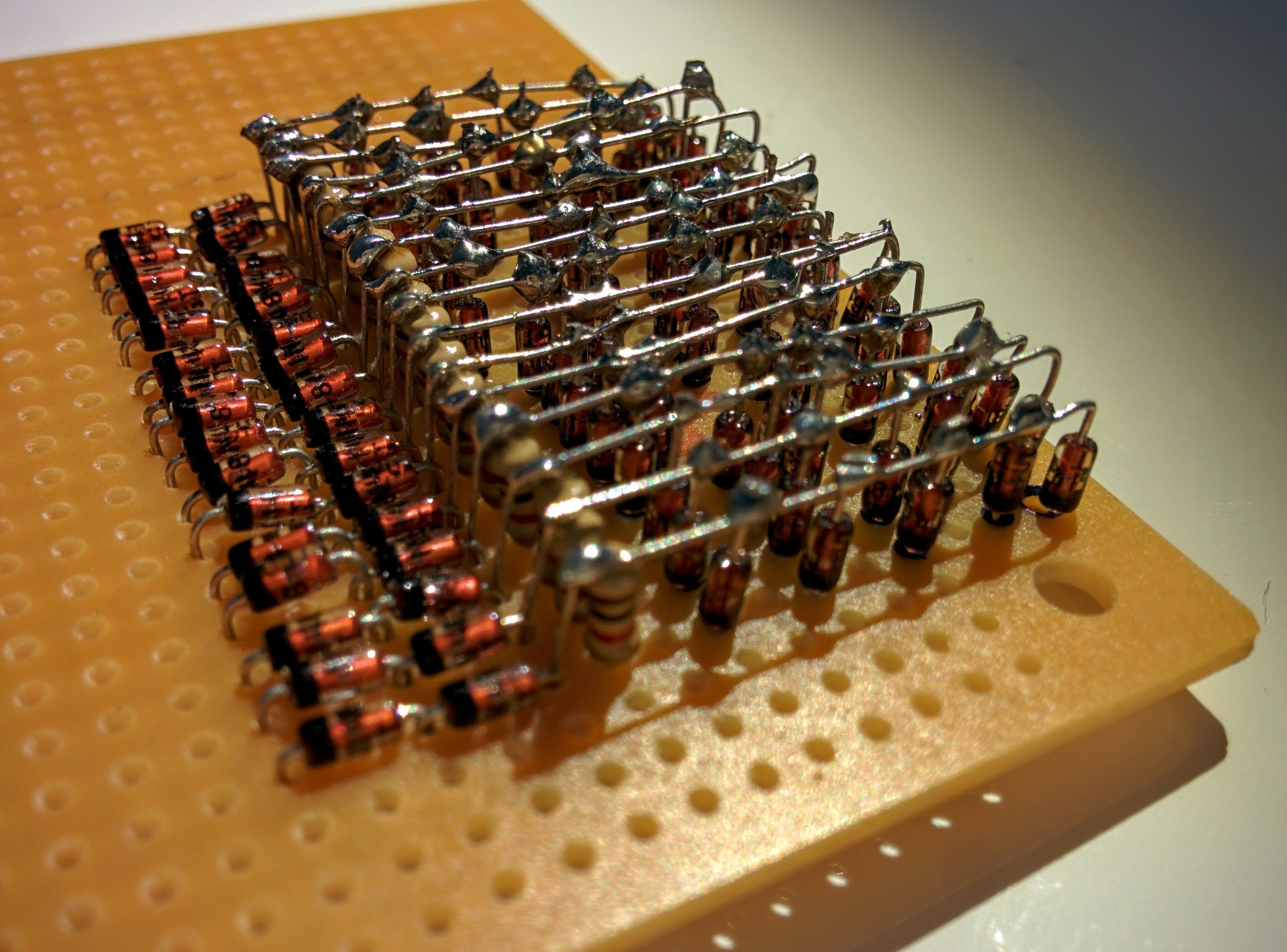
05/15/2016 at 11:29 • 0 commentsSince I'm moving overseas again I've had my lab boxed up and put in storage for the last few months but hopefully I can continue this summer again. I'm looking forward to actually do some soldering again after being forced to just hack around in software since last winter.
-
Four phase clock generator
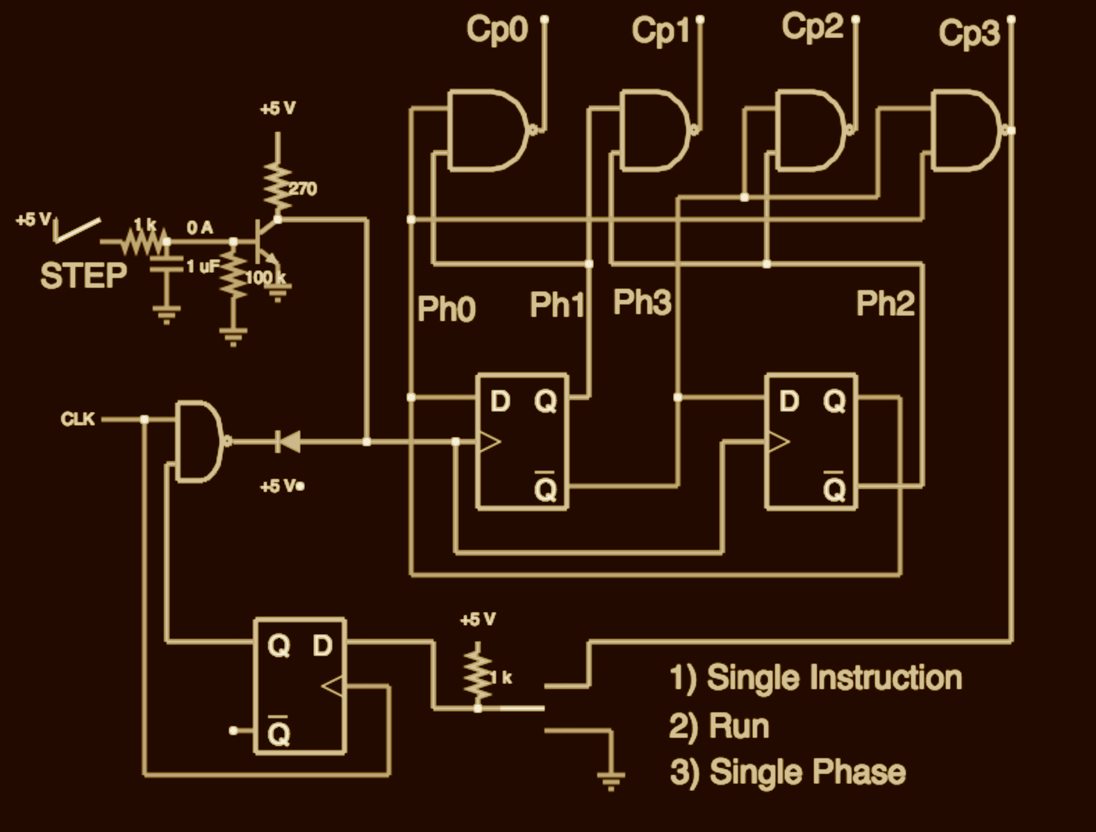
08/26/2015 at 06:09 • 0 commentsI'm not 100% sure of what I will need in terms of system clock, but this pcb will hopefully satisfy the needs.
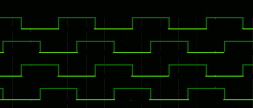
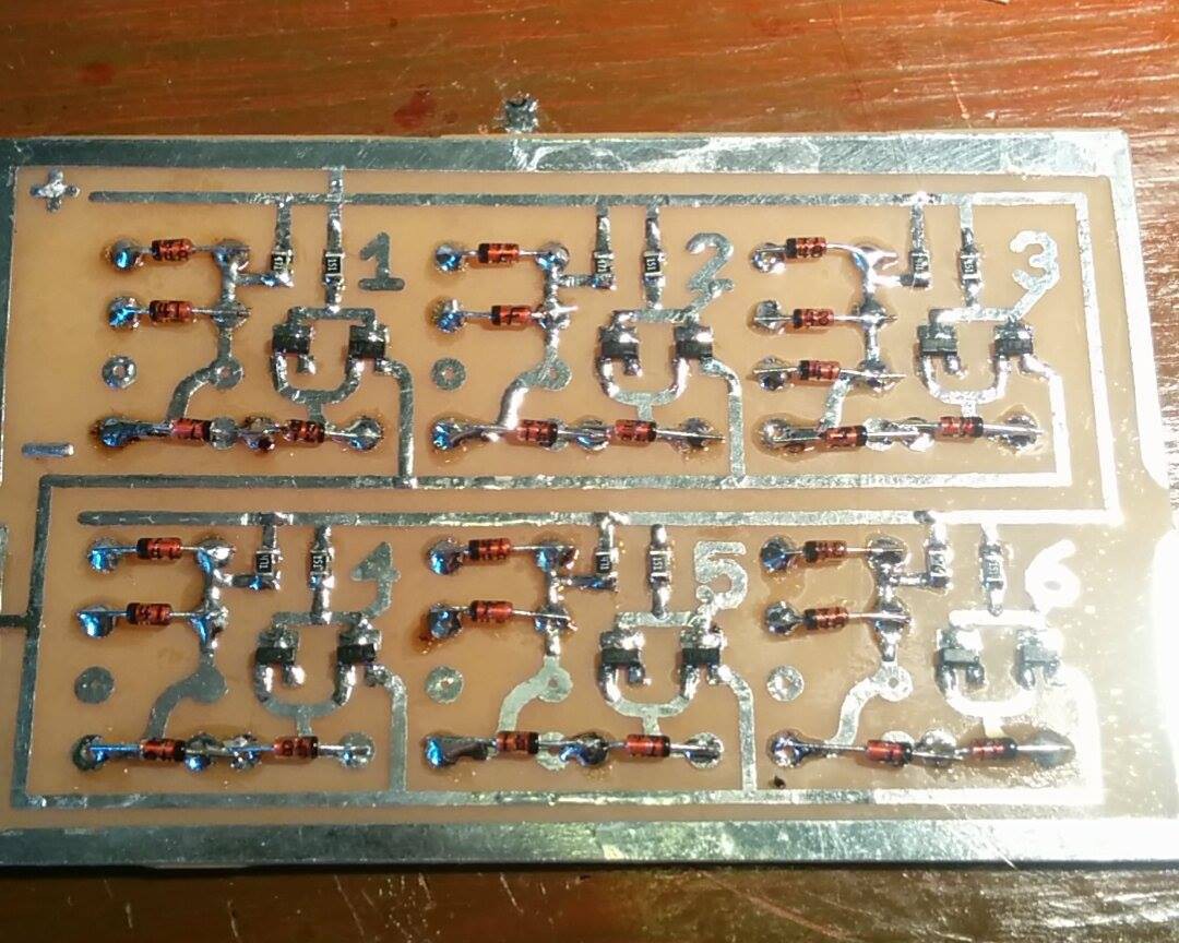
It outputs a four phase clock and can either be running normally or single stepped per phase or single stepped per instruction cycle (all four phases per step)
![]()
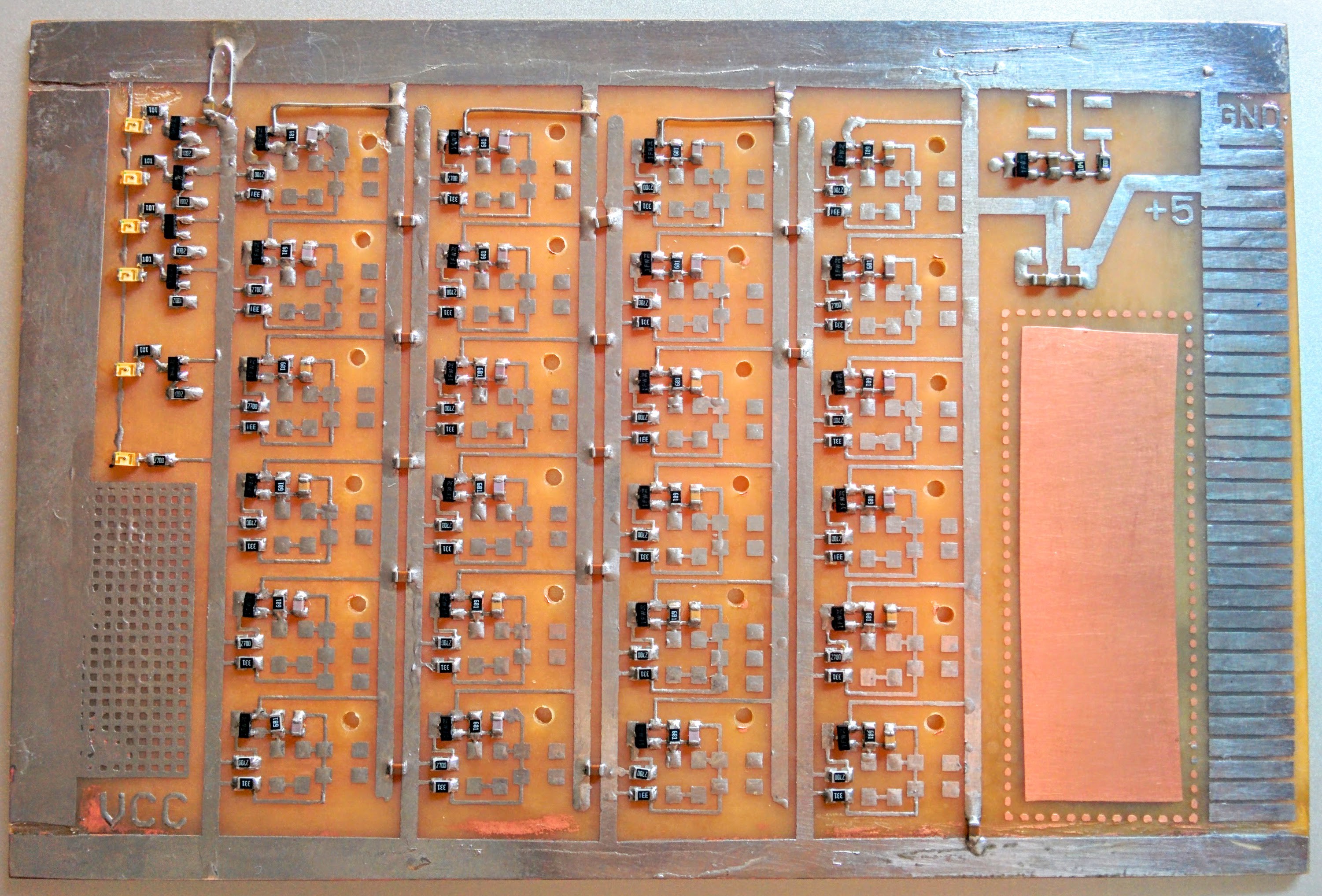
I'm still waiting for a delivery of SMD diodes to finalise the soldering...
![]()
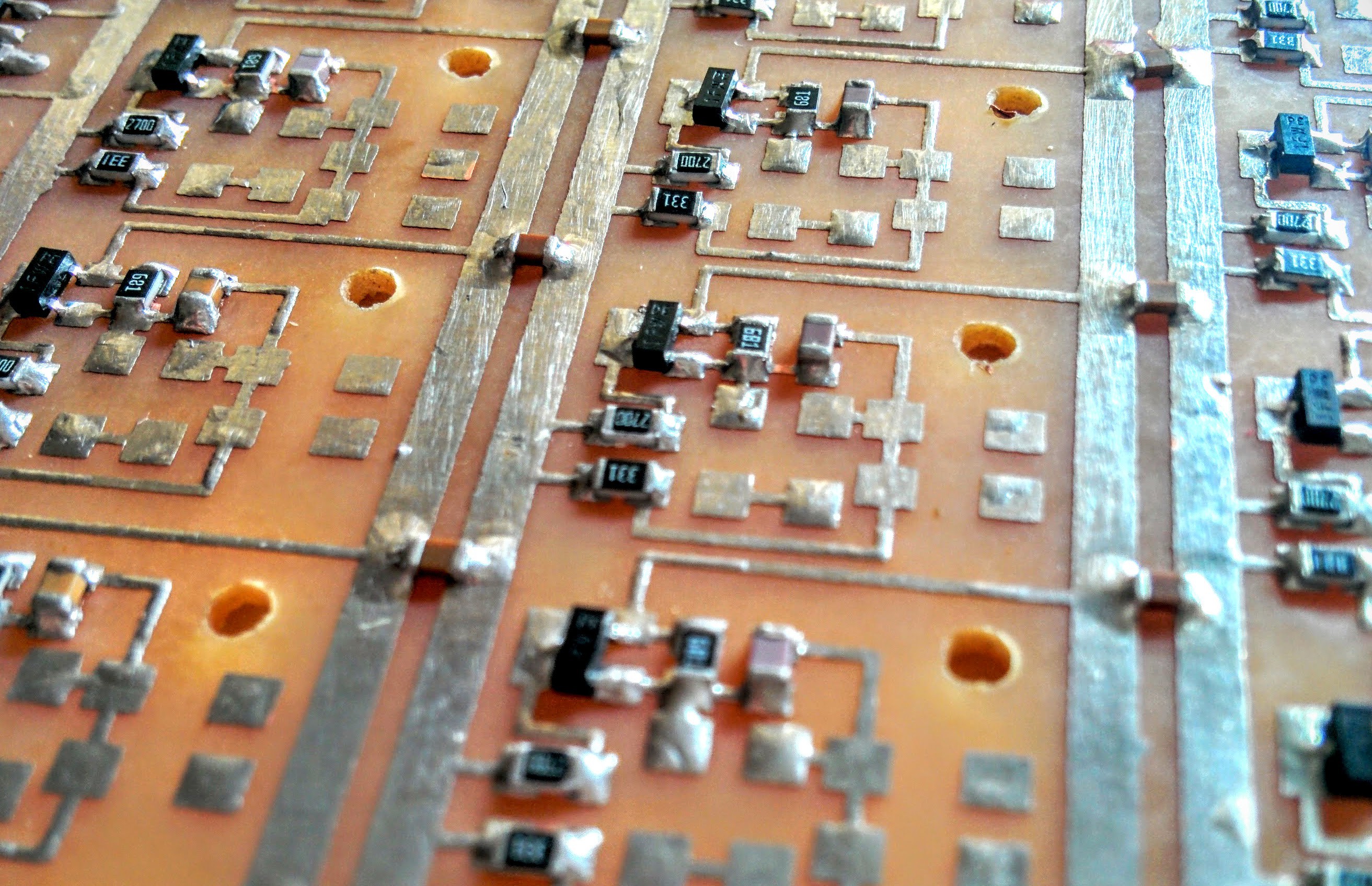
The routing between the individual nand gates will be done at the backside of the board with the wires coming up and going down in the nearest hole.
![]()
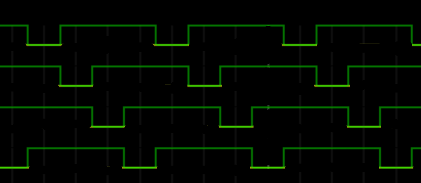
The board generates two types of four phase clocks divided down from a master clock (a 8 MHz transistor based Pierce oscillator that will be built Manhattan style on the empty space of the pcb)
![]()
![]()
-
More speeeeed!
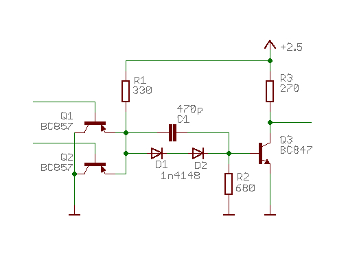
08/23/2015 at 03:55 • 4 commentsI redesigned the individual NAND gates a bit now using a PNP's as the input diodes, a speedup cap over the diodes, a pulldown at the base of the output transistor instead of a Baker clamp and running it at 2.5 volts.
![]()
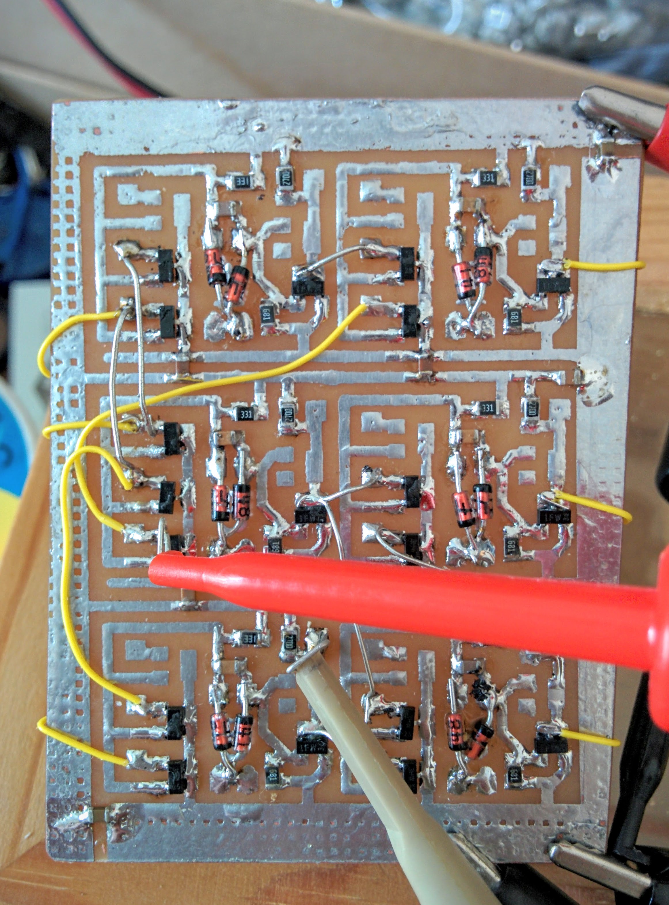
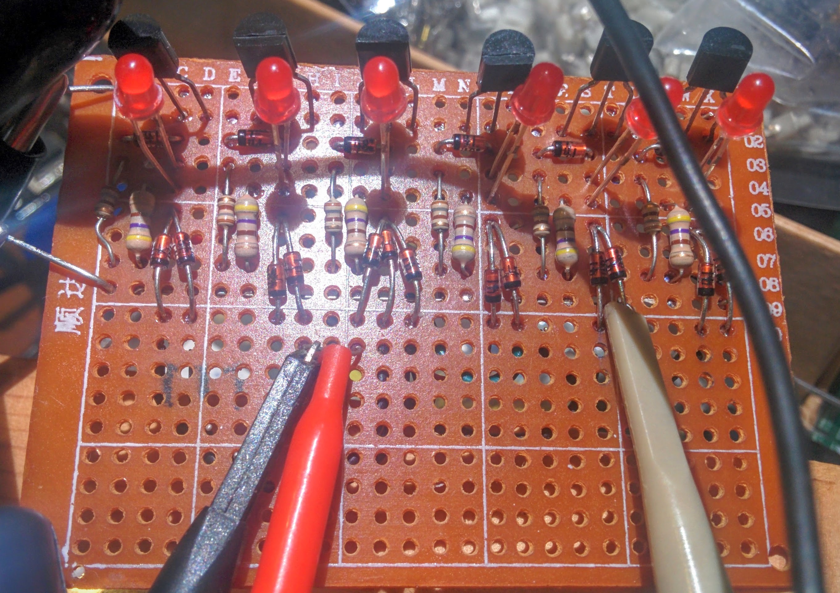
Soldered up and connected to the lab equipment it looks like this
![]()
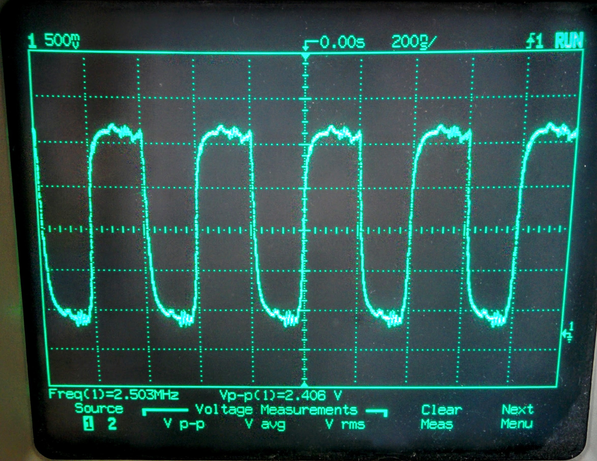
And if I feed it a 5 MHz square wave it actually outputs a rather nice 2.5 MHz waveform :-)
![]()
So now I have a design that is speedy enough to actually be used. From 180 KHz to 5 MHz in two days. Good enough for the time being.
The BC857 are a bit more expensive than small signal silicon switching diodes, so I think I'll experiment a bit more and see if I can't get 5 MHz with diodes on the inputs as well.
-
Testing speed of D FlipFlop/Counters
08/21/2015 at 13:14 • 3 commentsNow when I'm back home with a lab a bit larger than a single small desk I soldered up two versions of a edge triggered D FlipFlop.
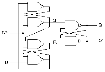
The general schematics for NAND based Edge Triggered D FlipFlip
![]()
The first version used a single LED as the level shifter and a silicon diode as the Bake Clamp. The second version is more standard, using dual silicon diodes as level shifter and a BAT54 Schottky as the Baker clamp.
When simulated in LTspice both version can (when configure as divide-by-2's) can work up to a bit more than 4 MHz. The LED/Si version was just a little bit slower than the 2Si/Sch, just a few % difference.
But in real hardware the story was quite a bit different.The LED/Si version only worked up to 180 KHz at 3.3 volts, when lowered to 2.5 volts the max speed rose to 210 KHz. Very slow and basically unusable for building the four-phase clock generator for the CPU.
The 2Si/Schottky version did better. 550 KHz at 3.3 volts and 720 Khz at 2.5 volts.But this still about an order of magnitude slower than simulated. So I need to work on getting the speed up quite a bit before I send for any of the PCBs I've designed the last two weeks. :-(
The LED/Si version
![]()
The 2Si/Schottky version
![]()
-
One ALU Slice tested with real hardware
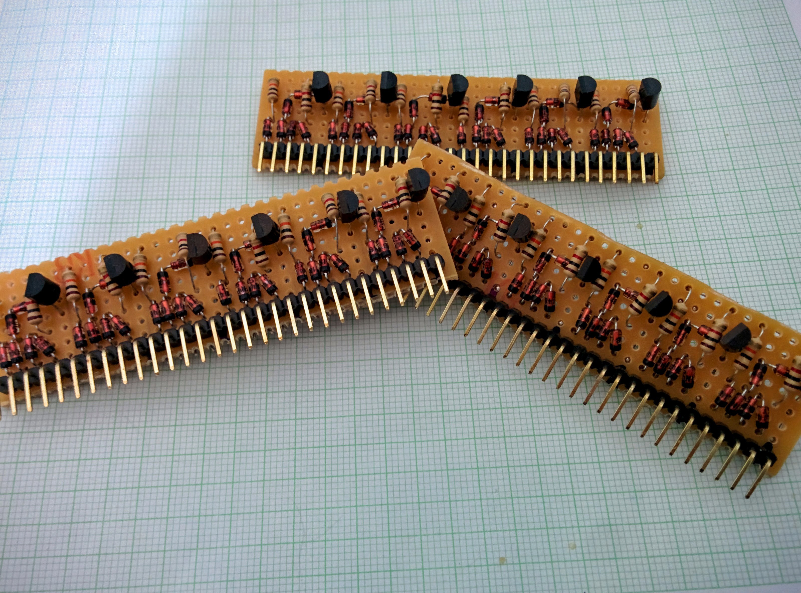
08/02/2015 at 17:22 • 8 commentsI did some soldering today.... Three boards each with six 4-input NAND gates giving 18 NANDs in total which is more than enough to wire up one ALU Slice and verify that it actually works in real life and not just in Logisim. The boards look a bit like the SIP (Single In Line Package) memory modules that was used for some years back in the 90's.
![]()
I realized that for the shift/rol instructions I need to be able to disable the Result and CarryOut ports of the ALU slices so there's now one additional control input to the slices and one more diode each for the two output gates.
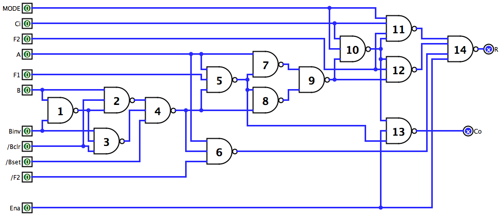
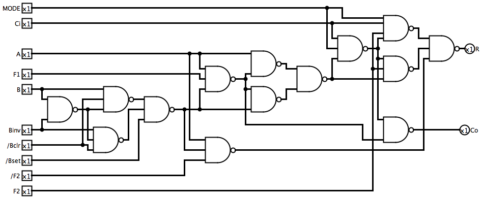
So a slice looks like this now:![]()
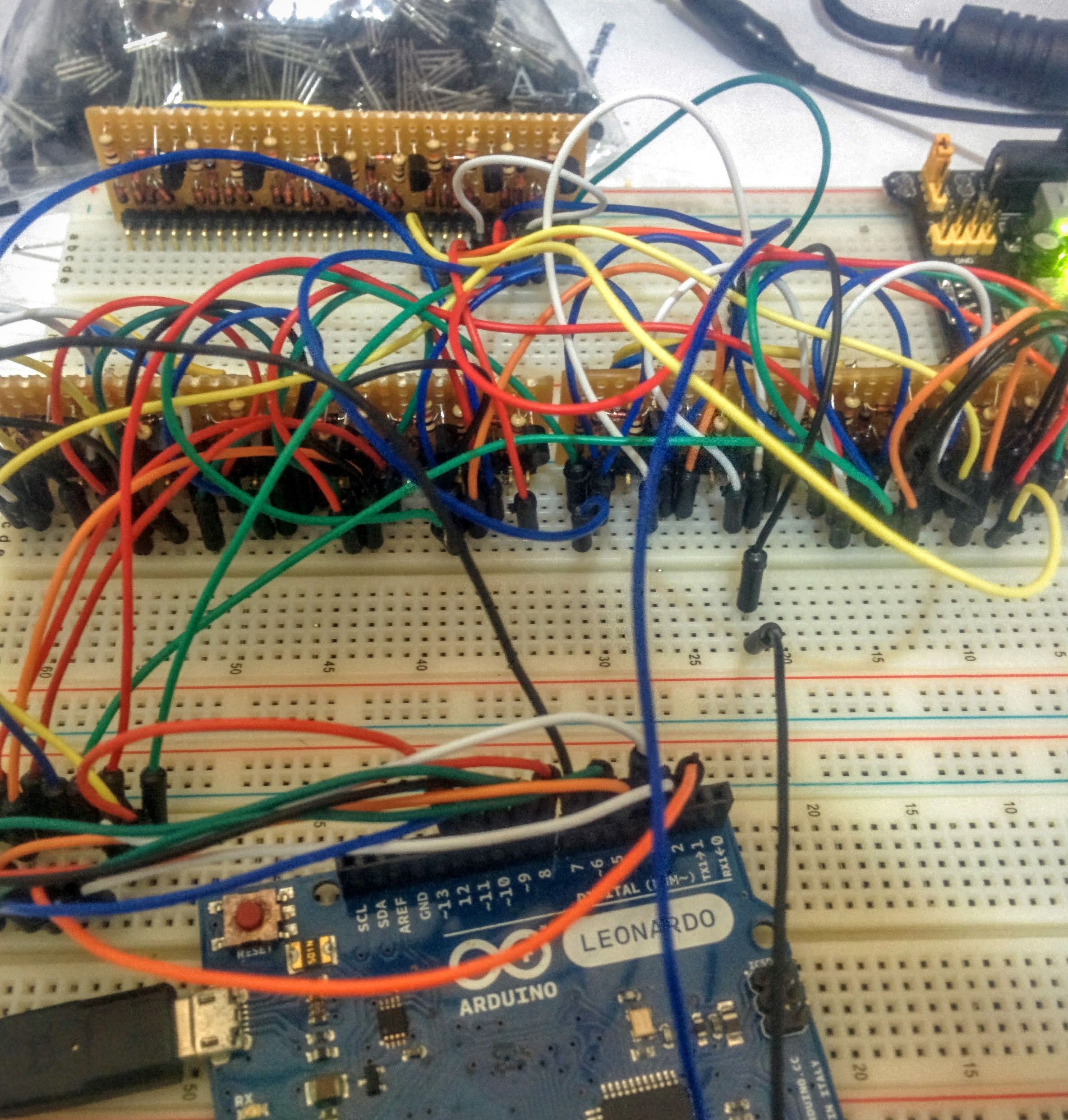
So I wired that up on a breadboard and hooked up an Arduino to automatically set the control signals and cycle through the combinations of A, B CarryIn and analyse the Result and CarryOut to see if the ALU behaves as expected. As far as I can see it does, so I'll route pcbs for this and send them off for manufacturing.
The ALU control pcb and the Shift/Rol pcbs I'll probably just solder up on breadboards since they're on-offs.![]()
-
ALU slice design done
07/30/2015 at 11:17 • 0 commentsIt took the better part of day, but but finally I've got a low transistor count version of a single bit ALU.
It does both arithmetic and logical operations and the result ends up on a single output pin.
Usually most ALU designs have a rather big multiplexer at the output stage where one of the results of the desired operation is selected. That would not be a big issue if using ICs, just a one additional chip would be required, but when building it from discrete NAND gates it's not that simple.
My ALU slice have the usual A, B and CarryIn inputs and a Result and CarryOut as outputs. In addition to that there are seven control inputs that will be shared among all slices that will be used in the complete ALU.
One of the control inputs are required both in a normal and also in an inverted version. I could have put the inverter inside the slice and then I just had to distribute six control signals among the bus. But I choose to put the inverter on the control pcb instead - thus saving seven transistors in total.
Depending on the state of the control inputs the ALU slice does the following common functions (plus a number of strange things that I'll don't have use for).
a AND b a OR b a XOR b NOT a a all 1's all 0's INC a DEC a a ADD b a SUB b
The ADD and SUB both have variants with/without Carry.So I ended up with 14 transistors, 38+(14*3) = 80 diodes per slice. Outside of the slice I'll have to add some logic for the shift and roll instructions as well. I think I'll implement them parallel to the A/B/Result pins since no arithmetic or logical instructions will take place at the same time so by bypassing the main ALU will reduce the propagation delay a lot.
![]()
I'll breadboard this up and connect it to an Arduino to verify that all ALU ops are correct before I design a PCB for it.
-
Feeling the pressure
07/29/2015 at 02:05 • 2 commentsThis project is starting to get a serious amount of skulls and followers which on one hand is nice, but on the other hand is giving me pressure to actually move forward in a decent speed - no slacking off here :-)
Well, just as an update of what I'm currently doing the last few days:
The emulator now loads code, sends logdata via udp and have a simulated UART on a tcp port.
I've also started working on the ALU bitslice for that can handle all 16 operations my instruction set mandates. I'm doing that in both in the simple Falstad circuit simulator for the overall view of it with logical blocks, and also on transistor level in LTspice to check timings/performance.
Hopefully the ALU design will be done this week so I can solder up one of the eight slices plus the control logic for it on perfboard, run some basic tests and then send for a full set of slice pcbs from dangerous prototypes after the tests.
-
CPU Emulator
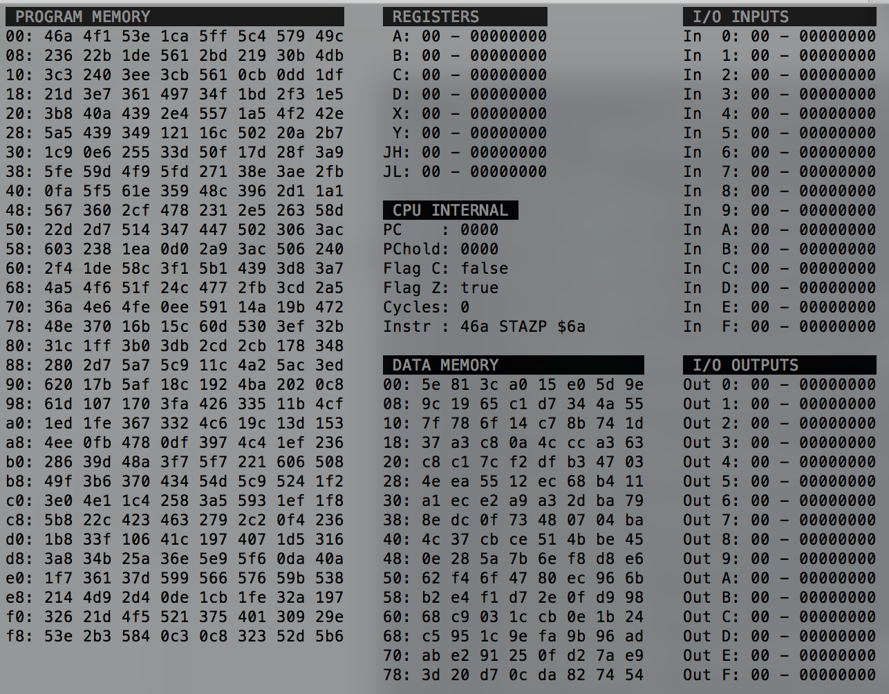
07/24/2015 at 10:45 • 0 commentsIt only took me about four hours to whip up an emulator for the CPU using golang and a library called termbox to handle the output to the screen (it's a lightweight version of curses). Since I'm an old C programmer and this is only my second golang application it probably have a lot of ugly C-mannerisms in the code - but it works and can execute the code I fed to it.
I still need to implement some rather important functions like Load code from file and Edit data in the code- and data RAM spaces.
It could also be nice to have a simulated serial port/uart on a tcp socket that can be telnetted to.And highlighting of fields that have changed during the last executed opcode as well - that would look very professional :-)
So a couple of hours more tonight to finish off the emulator....
![]()
-
A 4-to-16 decoder board
07/21/2015 at 11:17 • 0 commentsI've soldered up a 4-to-16 line decoder pcb. Two of those are required for the program address (ROM) bus, and at least two more for the data address bus (RAM).
I will have up to sixteen ROM boards each holding sixteen (11-bit) words of memory.
In order to not require local decoding of the last four address bits (A0..A3) on every ROM board I have a board like this that takes four binary bits and outputs one of sixteen select signals that goes out to a bus that all ROM boards are connected to. Then each ROM board will have a separate board-enable signal as well - or all boards would respond at the same time.
This decoder board is basically just five inverters (A0..A3 plus Enable) that is connected to sixteen 5-input NAND gates that are then followed by sixteen inverters that goes to the outputs of the board.
In total I ended up with 139 diodes, 50 resistors and 41 transistors if I've counted correctly.
I think I'll have to draw some block diagrams to explain the workings of all my pcbs and how they will be interconnected....![]()
![]()
-
Assembler for this cpu
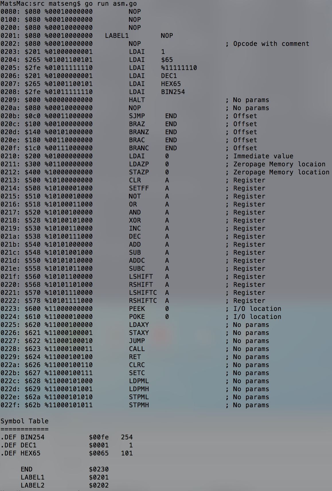
07/20/2015 at 11:13 • 0 commentsThis weekend I didn't have time to hack at the hardware, but I started writing an assembler for the cpu.
Being a old C programmer I decided to try my hand on a another language to challenge my hacker spirit. I've wanted to use golang for something for a while now, so I spent a few hours picking up the basics of the language and then another few hours to implement the basics of a two-pass assembler that can process the instruction set of my cpu and some necessary directives like .def and .org.
I must admit that it was a piece of cake - much easier than I anticipated. The functionality of the assembler is not 100% yet, but gimme another hour or so and it will be done. :-)![]()
AYTABTU - Discrete Computer
After the apocalypse we have to build computers from stuff we can make at home, I.E Transistors, diodes and resistors.
 matseng