 SHAOS
SHAOSIt's time to explain experiments that I performed on actual 1801VM2 in February (some pics were in gallery since the beginning of this project without explanation). So it is important to know that most of VM2 pins have to be pulled up to +5V through resistors (I used 2K):
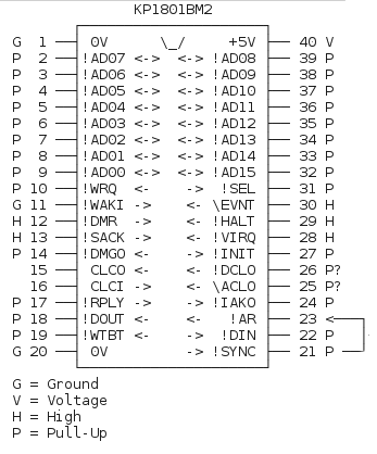
Here everything marked H and P are pulled up. G is grounded and V (pin 40) is actual +5V line:
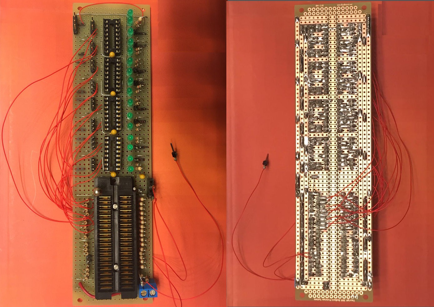
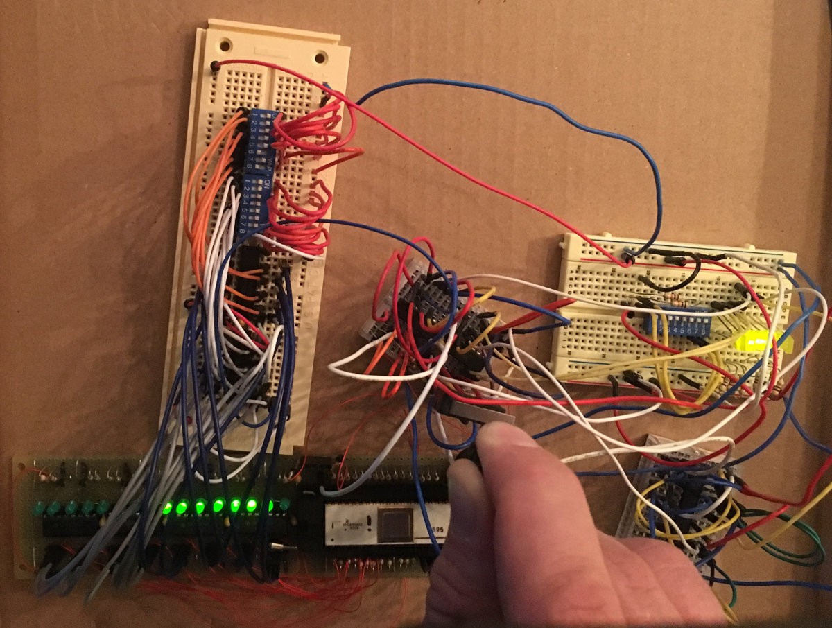
Then I decided to build a simple circuit to test VM2s by manual clocking through not existing memory (later I added a NOP instruction 0240 that is hexadecimal 0x00A0). Also PDP-11 architecture assumes a special handshake during reading and writing to support slow peripheral devices - on every !DIN and !DOUT external device must produce !READY triggered by !SYNC otherwise processor will go to trap subroutine after some number of cycles, so this is schematics that use three 74LS00 to generate !READY (without a delay - as fast as possible) and indicate on LEDs some important signals:
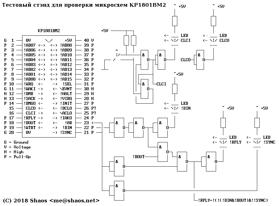
Clock is generated by manual pressing a switch button (because 1801VM2 has fully static design and may handle 0 Hz frequency) that goes to simple RS-trigger and then to CLCI input (pin 16) and indication through inverter (LED CLCI). CLCO output (pin 15) is CLCI frequency divided by 2 - it goes to indication as well (LED CLCO). 1801VM2 added another handshake that doesn't exist in PDP-11 - !AR that must be returned everytime when device catches address in the beginning of !SYNC - for simplicity !SYNC and !AR could be directly connected (see above pins 21 and 23). !SYNC goes to indication through inverter (LED !SYNC) and also used to generate !RPLY (pin 17) with help of !DIN (read control signal on pin 22) and !DOUT (write control signal on pin 18):
!RPLY = !(!(!DIN&!DOUT)&!!SYNC)
NOTE: In real application with interrupts also !IAKO should be used here, but we don't have interrupts for now so this simplification should be good enough to start.
Another handshake from PDP-11 is special procedure to power things up - after switching power on 2 signals !DCLO (BDCOK H in PDP-11 world) and !ACLO (BPOK H in PDP-11 world) must be low. Then !DCLO goes Hi (at least after 5 clocks CLCI from power on) and then !ACLO goes Hi (at least after 10 clocks CLCI from !DCLO went up) - here I simply used 2 grounded wires that I manually connected to pulled-up pins 25 and 26 in proper order after some number of clocks.
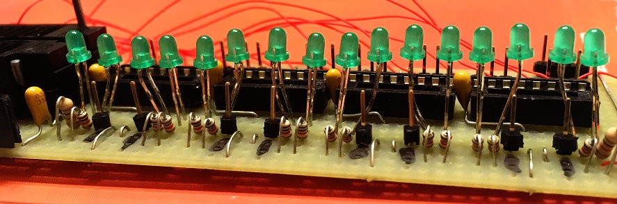
Also I added address latch on 4 chips 74LS75 that stores address from AD lines in the beginning of !SYNC to show it on LEDs and use in future when actual memory is connected:
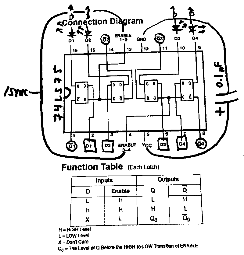
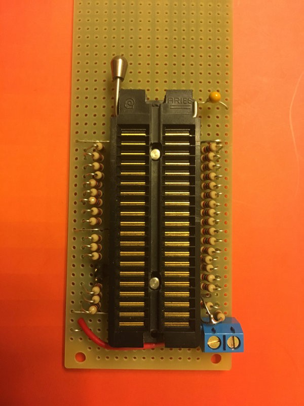
Here D1-D4 are four AD-lines from VM2 and !Q1-!Q4 are inverted latched address bits that were inverted so it's not inverted anymore (and Q1-Q4 go to indication and stay inverted). This is a board with ZIF socket (and I should be honest - inserting Russian chip with metric pitch there was a little problematic):
First test (circuit was even simpler that time - it used only 2 74LS00):
I put results of initial start in Wavedrom to make it more visible:

You can see !DIN goes down 3 times - 1st time without !SYNC when it's reading starting vector from external circuit - because nothing is there and AD lines are pulled up it reads 0xFFFF inverted or 0x0000, so it assumes that starting address and flags are stored in address 0x0000 so then it reads address as a word from 0x0000 (2nd !DIN) and then flags as a word from 0x0002 (3rd !DIN).
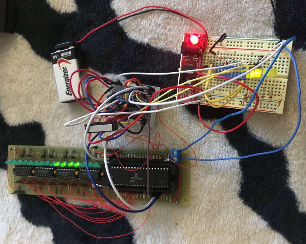
Then I added 2 buffers 74ALS240 with 16 switches to imitate memory response on reading to have NOP instruction 0240 (hexadecimal 0x00A0) be on data bus when !DIN is down to turn VM2 into counter:
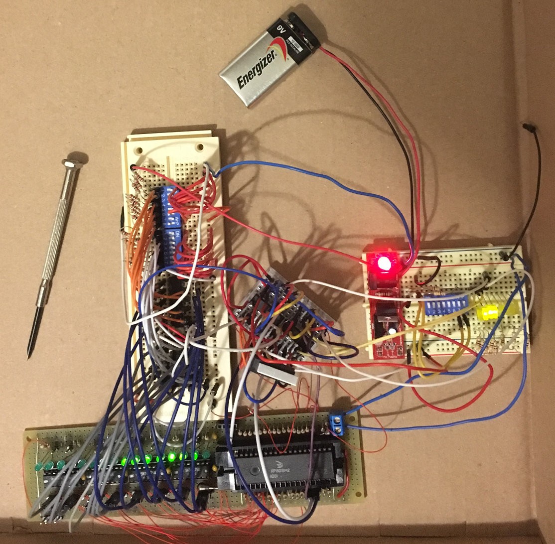
At this point I was able to test all my VM2 chips - I assumed SUCCESS if chip was able to run at least to address #00FE (0000000011111110) - as pictured above. So from 4 black (plastic) KR1801VM2 (КР1801ВМ2 1992 & 1993) ALL were good! But, from 6 white (ceramic) KM1801VM2 (КМ1801ВМ2 1989 & 1990) only ONE was good :(
TO BE CONTINUED
Discussions
Become a Hackaday.io Member
Create an account to leave a comment. Already have an account? Log In.
Really love the idea of bringing old CPUs from decades ago to life and see if they still work (odds are, they do! :-)) I have a beautiful ceramic KM1801BM3 (manufactured: 9003) which I would like to test, my idea is to put it on a breadboard and bring signals to it using FPGA. Somewhat reverse of this project: https://hackaday.io/project/182959-custom-circuit-testing-using-intel-hex-files
Problem is, I can't find much about this fancy processor at all :-( Basic data sheet with pinout and bus cycle sequences / time diagrams would be helpful. Any pointers where I could find it? Russian is fine, I can read Cyrillic and understand a tiny bit at least to the extent of know what is what.
Are you sure? yes | no
VM3 is much more complex machine - you can find some docs in Russian I guess
Are you sure? yes | no