Aditya Mukherjee
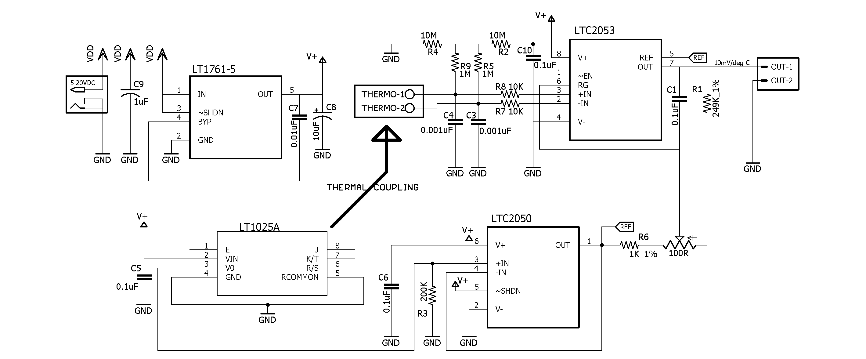
SCHEMATIC
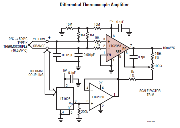
While browsing the LTC2053 datasheet we found a neat little schematic shown here, which only needed a properly regulated voltage supply.
The default gain for k-type thermocouple of the circuit gave us an output of 10mV/degC which was ideal for us so we did not have to change any values.
Know more about thermocouples.
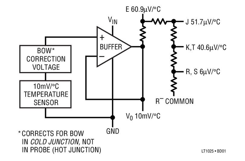
Along with the temperature coefficient of the thermocouple we also need to know the temperature of the cold junction. Thermocouples sense the temperature of its tip with respect to the cold junction temperature which is the junctions between the thermocouple terminals and the circuit board (green screw terminal in this case). We can ignore this whole fact only when the cold junction is precisely 0 degC, but in most of the cases its either room temperature or some non zero temperature, in that case the output will have an offset equal to the voltage corresponding to the room temperature (10mV x room temp).
We could always dip the tip ("dip the tip" - try saying that fast .. haha) in an ice bath and calibrate the device..... but ... why ? We could just throw in a cold junction compensator (LT1025), which ... yeah right !!... does all the hard work for us. It does not only set the zero point precisely but also calibrates the device pretty well and corrects non-linearity in the thermocouple output graph.
The thermal coupling in the first schematic is needed to keep the cold junction and the CJC at the same temperature.
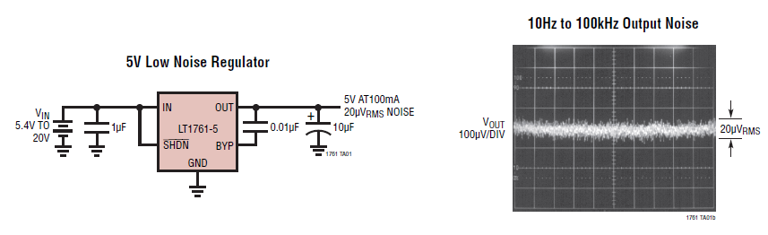
For the regulated power supply we used LT1761ES5 low ripple 100mA 5V reg. Avoid using cheap power supplies in precision circuits, it will almost surely screw things up at some point.
FULL SCHEMATIC
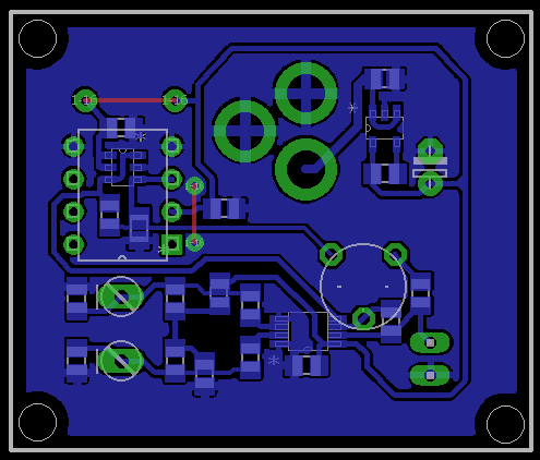
BOARD LAYOUT
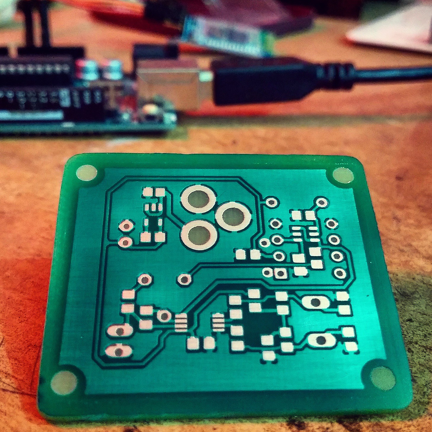
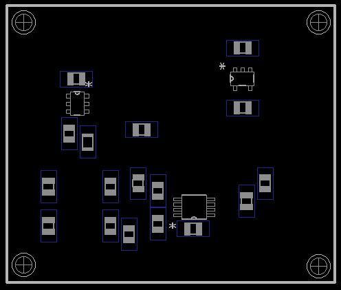
The PCB was self fabricated so to keep things neat and simple, the design was made such that only one layer of copper was needed.
All the SMD components were on the bottom layer and all the through holes on the top.
While designing in eagle keep in mind to press the middle mouse button to flip a component from top to bottom layer and vice versa, Don't punch your monitor if the pcb is fabricated with mirrored pads ^_^ .... just saying.
Though I am not a huge fan of jumpers on a PCB (defeats the whole purpose of making a PCB) I had to use two of them .... -_- . Anyway.
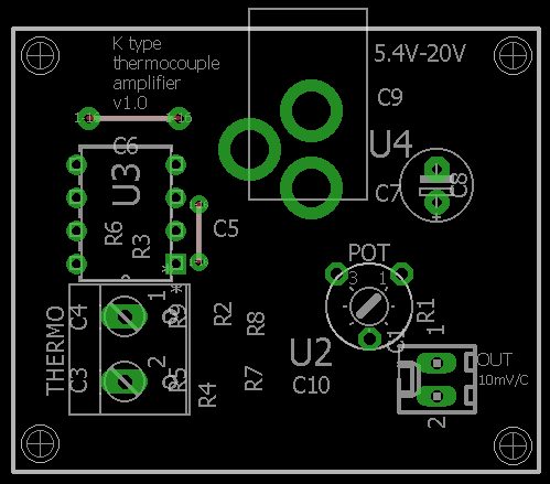
Notice that the screw terminal is placed adjacent to the CJC (LT1025)
All board design files are in the github repo or the files section over here.
FABRICATION
1. First cut out a rectangular piece from a single sided copper clad board which is slightly larger than the PCB dimensions and file off the sharp edges.
2. Rub off the impurity layer from the copper with a metal scrubber (till its shiny) and clean it afterwards with alcohol (IPA).
3. Apply photo resist film on the cleaned PCB
4. Place the negative photo mask of the bottom copper layer on top of the film and keep the board along with the film and mask in between two glass slides so that the mask sits evenly.
5. Expose the film under UV light (time depends on your UV light strength, I use a nail polish hardener and it takes me 1 min).
6. peel off the second protective layer from the film and dip the board in developer solution
7. After the board has successfully developed etch the board in FeCl3 or whatever you use.
8. Clean it up and apply UV curable solder mask paste (or if you have film .... I'll take it off your hands) and place an OHP sheet over it to even it out.
9. Place the transparent solder resist mask and expose for a longer time (it takes me 8 mins).
10. Peel off everything gently and wash the board with alcohol, it will remove the solder resist paste from pads and vias, sometimes it requires rigorous cleaning, don't be afraid to put some pressure.
11. Drill the holes...................Done !