 Antti Lukats
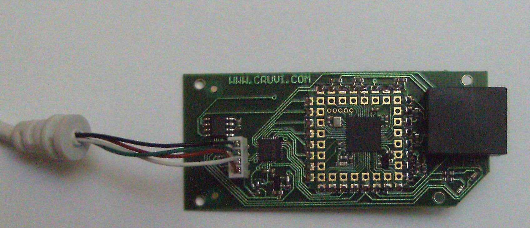
One predecessor of the #DIPSY is this Actel-based prototyping/OEM board.
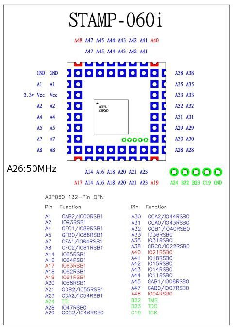
It may look trivial to build, but it uses the CN132 package of the Actel (Microsemi) ProASIC3 FPGA family. This is one of the worst packages: it is 3 row staggered QFN style package with 0.5mm pitch.
This is near to imposible to get it routed for 2 layers using PCB technology for low cost manufacturing. To my surprise the factory in Taiwan had almost 100% yield with this board.
The trick is that not all the pins are available. Only those that can be "escaped" have external pads. The small size limits the number of pads anyway and 30 GPIO is already more than necessary for many simple applications. Why use a microcontroller when you can reconfigure any pin to do anything at 50MHz ?
The FPGA was pre-programmed with soft-processor based on AVR Instruction set. Of course that was only the "demo" image, the FPGA was reprogrammable in system, the small holes are JTAG.
IMPORTANT: This is completed project, and it is not possible to produce any more 100% same PCB any more as the FPGA in this package is no longer available.
@Yann Guidon / YGDES still has some boards left (for his own prototyping needs) and uses this page to keep the documentation online, now that Mirifica (the last distributor) has shut down the archives.


 marble
 Collin Matthews
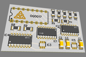
 macafeeje
 Viktor Nikolov
These tiny boards are not very powerful but so handy !
I'm using two right now for the v1.5 of #Rosace and they save my sorry a$$, once again !
Thank you again Antti !