 DrYerzinia
The PCB is now at revision 7 and getting ready for a final professional prototyping build and the case design is still very much up in the air right now.
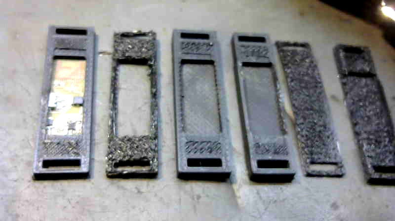
I printed 6 different cases based on the threaded through collar design. The first 2 I printed with flexible filament. The first one printed ok, but after that I couldn't get the filament to feed right in my printer anymore and gave up on it. Instead I printed 4 more out of PLA to make sure all the dimensions where right and everything fit. Turns out I had some things wrong. The first thing was the side walls where too thin. Turns out my openSCAD equations weren't right and I was subtracting to much. The I realized I had my buzzer/microUSB holes on the wrong sides as well as it being a bit thicker than I wanted overall.
My printers z-resolution is better than its x or y so I trimmed down the front back thickness to 0.7 mm. The wall sides need to be atleast thick enough to have 2 layers of PLA so they are set to 2 mm thick. I left 0.35 mm for the edge of the solar panels to slide into their pockets.
The board sits in there pretty well but I realized with it thinner than the overall case the micro USB can't protrude one side while the buzzer is flush with the other. Since the r7 board is going to be 15 mm wide and the battery is 18 mm wide there is no way to reconcile that from case changes. Right now I'm planning to change batteries to solve the problem. A 2x12x12 mm battery that will sit over the power supply circuitry would allow it to be about 0.5 mm thinner and still retain most of its flexibility. Then I can match the width of the case to the width of the board and have the buzzer and micro USB both be flush.
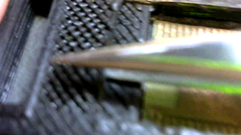
The way I'm printing now I can't fit the solar panels into the pockets in the case because the layers fuse together during printing. For this to work I will probably have to pause printing before this layer and insert the circuit board and solar panel. Then the printer can lay down the top layer over the flaps and seal it in.
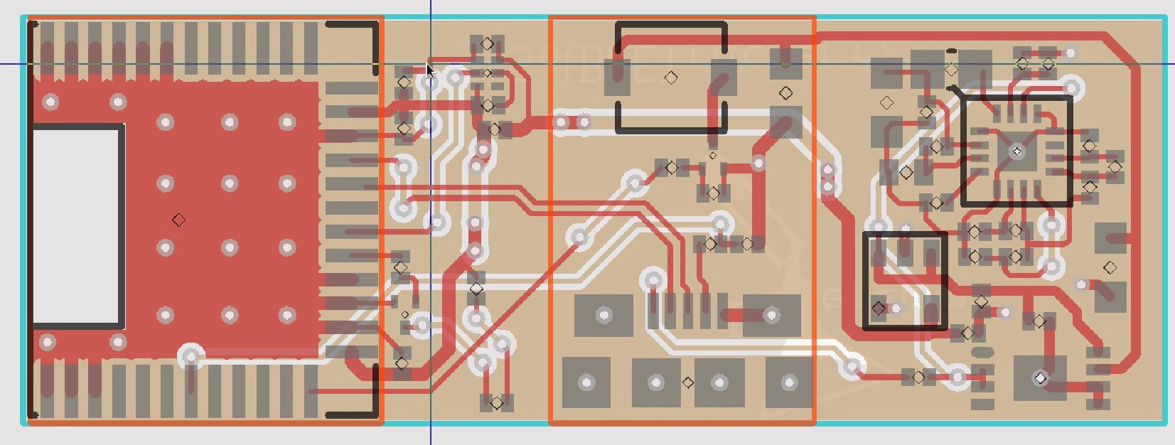
On the revision 7 design of the PCB I upgraded to using 2 layers. The difference in production costs is insignificant and it allowed me to narrow the board to 15 mm as well as add a nice ground plane and clean up some of the traces.
All the power trance now have some width to them even though that's likely unnecessary and anywhere a part needs a ground it can just drop down to the bottom layer. The RF performance of the BLE121LR should also be improved by the larger ground plane.

The last thing to look at is the testing of the collar. Right now I have one deployed in the field on Jasper. It spent a week in the basement on the pool table and is still running fine. Now its chilling out on Jaspers neck. Its been there for a day and still working. This version is using the thin curved PLA case construction. The circuit board is pretty much hanging out in the breeze but it seems to be holding up just fine.
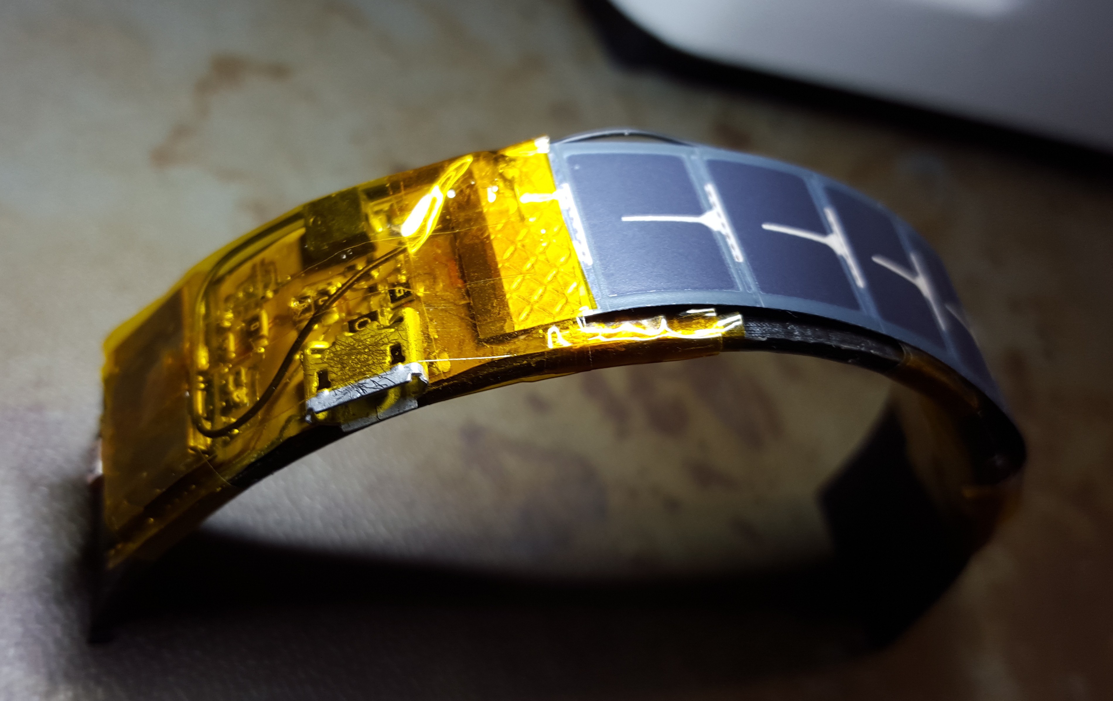
Everything just looks better with Kapton tape on it. That gold sheen makes it look like its meant to go out exploring in the vacuum of space!
Discussions
Become a Hackaday.io Member
Create an account to leave a comment. Already have an account? Log In.