 ben biles
I recieved my first DSP Mixer board today from www.pcbway.com/b
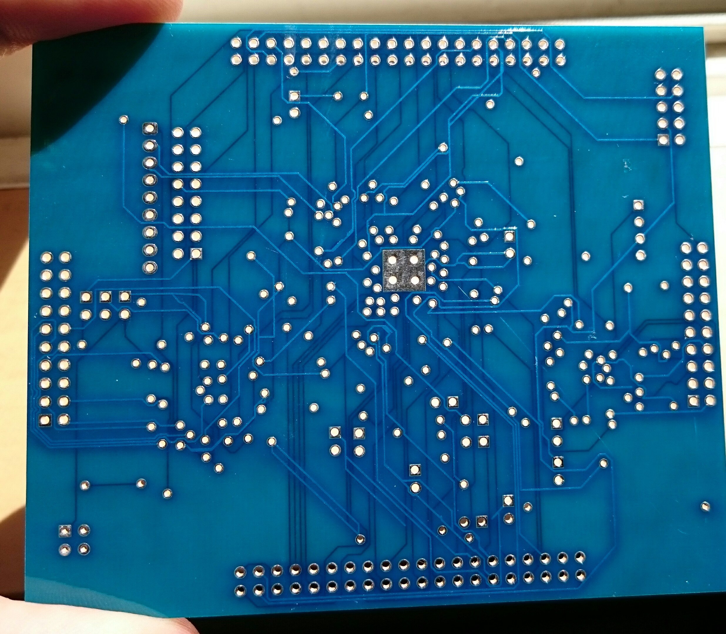
its my first 4 layer board so I was a bit nervous I had done the layers properly. when I held it up to the light I could only see 2 trace layers so thought uh oh !!! but got the continuity tester onto it and all is fine so far :)
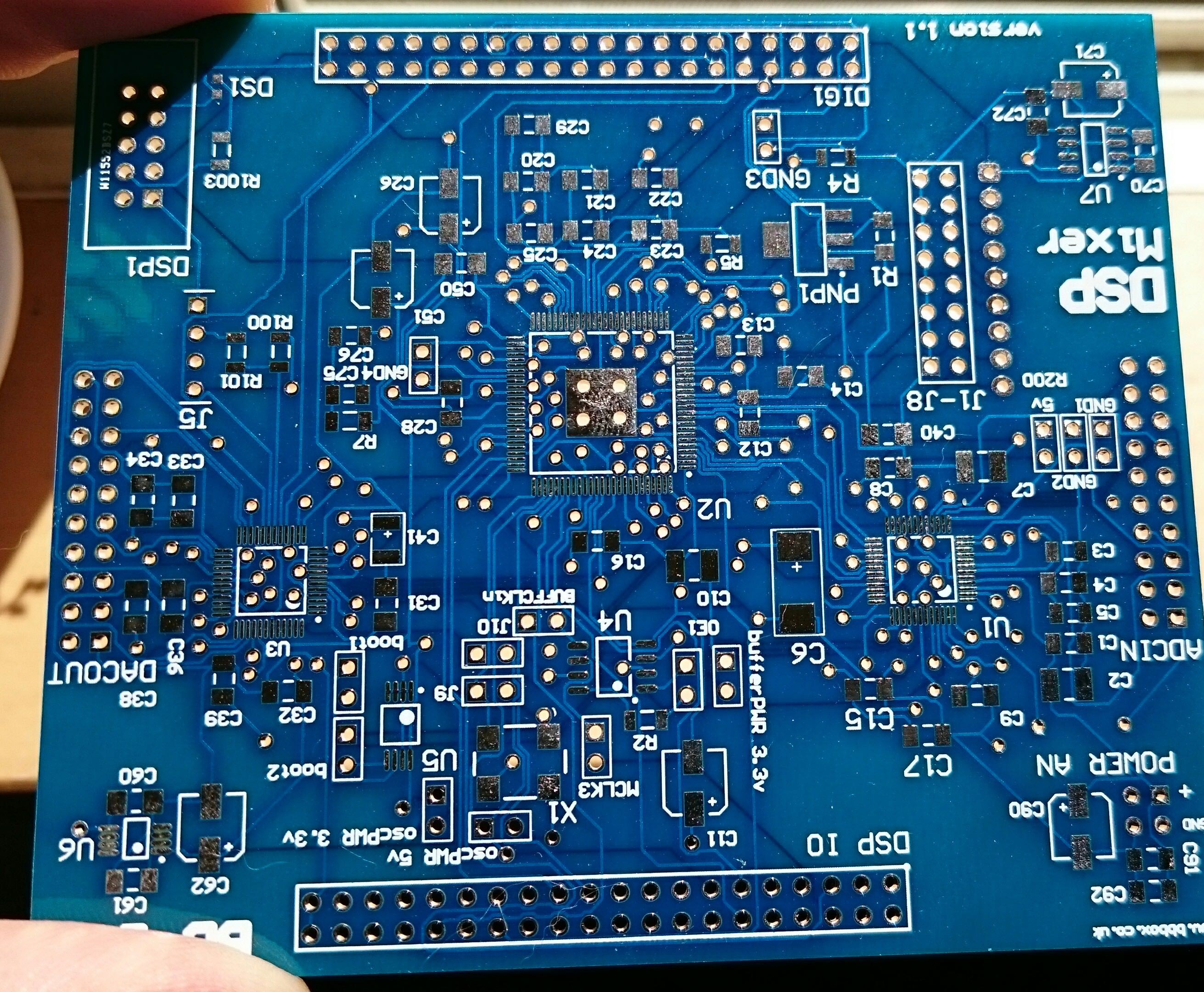
I can't say I spent too much time making the perfect routes on this board. I tried to keep the analuge stuff away from the Digital traces as much as possible. its more of a proof of concept board tham a finished design.
PCBWAY where the cheapest place I could find for a 4 layer board of this size. I had a ton of vias and pads and there was no penalty for it. next revision of this board i will use smaller vias as advised by people in the comments below :) I'll also try to use a power plane and ground plane of 3.3v.
However I think I will need to go up to 6 layers of I want to keep the boards 10x10 size. This seams to be PCBWAY's cheap prototype size.
if the 24.576 master clock with fan out buffer works fine between all the ADC DSP and DAC then and it works , then I will re-design the layout better.
 I have a lot of vias very close together , and some things are down to 6mil ! Also I found in circuit maker I had to disable loop checking ( via's were randomly dissapearing from the design ! )
Anyway, the board looks for the price a decent quality. I find that if you keep a 4 layer board with 10cm x 10cm the price is ok.
I was going to go for a full mixer board with analouge and DSP mixer in one but decided to keep things sepperate for now and do more testing. mainly with RC filtering between the analouge driver between ADC and DAC. so there in no filtering with analouge IO on this board. Just naked IO pins from ADC and DAC !! living dangerously :)
I'll post some more pics here when I solder up the board and make a video of the thig working, if it ever does :) I did test a IDT fanout buffer before on vero board so hopefuly my traces are equall enough distances and not too far appart to not have problems with clock skew etc..
Discussions
Become a Hackaday.io Member
Create an account to leave a comment. Already have an account? Log In.
I have never used PCBWay before, for prototypes I use Seeed Studio Fusion service https://www.seeedstudio.com/fusion_pcb.html since a year. Quality is very good, I was also impressed with the shipping from China, as it was no more than an additional week with DHL.
Are you sure? yes | no
This is Anson,thanks for share www.pcbway.com/b ,your project is great,has given the skull
Are you sure? yes | no
It seems to me that the vias could be smaller, most PCB fab can drill much thinner holes. This will also help your routing. Check the fab's requirements, this will help you a lot :-)
Are you sure? yes | no
Thanks , thats some good advice !! I had a really hard time fitting the vias under the chips. did'nt think of reducing the via size at all but I'm sure its possible ! Also some of the vias are way to close for comfort to other pins under the IC's basically 6mil ! I did though manage to get most of the caps near the IC's but I am deliberately using larger 1206 passives and there are way too many jumpers for testing.. most of those will go in the next design.
Are you sure? yes | no
You can easily use 0805 caps to save room, 0603 if you're fit and 0402 is around the corner (needs some patience though)... I used 0603 and 0402 for the #WizYasep board, only 2 layers. Minimal size vias came to the rescue too!
Are you sure? yes | no
I like to push PCB vendors to see what they can do. I have to cut back on the fill isolations and silk screens alignment is when my Chinese PCB CM that my supplier use tends to slack off.
https://hackaday.io/project/4993-dual-channel-battery-chargeranalyzer/log/17291-keeping-up-with-the-times-prototyping-with-qfn-and-bga
Are you sure? yes | no
I will use smaller 0805 next time I think , I found on my last 2 layer board it was really useful to have larger pads, that way I could solder on through hole parts / bodge wires just to test things out if needed. I think if I get rid of the jumpers , went to 0805 / 0603 used power / GND plane for 3.3v I could get the board smaller. for testing things out I prefer the larger parts and pads though.. but , I will definately try the smaller Via's on any board I make in the future ! think that would save a lot of trouble especially under the IC's
Are you sure? yes | no
Yes , well spotted :) It definately is a 4 layer board and its definately not normal ! your absolutely correct ! I have no power planes , only traces. I'll do a screen grab from circuit maker and post it later so you can see the routing mess :) I have a ton of jumpers on the board and most of the passive componants are 1206 or larger. If the design concept works well with the multichannel pre-amp board ( that board is a 2 layer ! ) then I will prbebly try a 6 layer with internal ground planes. The board has sepprate GND's for analouge and digital so will need to be worked into the final board. I think I will need to split the GND plane into 3 but have no experience in doing this yet. 2 analouge ( 1 each side of the board for analouge IO ) and one center digital GND plane. not sure how or where i would connect the two analouge planes or how.
Are you sure? yes | no
I found it surprising to see a 4 layer board without internal planes as I manage to route my projects in 2 layers while keeping a ground plane under my tracks as a return path. The time I can't, I have return paths on the same plane and stitching a grid together.
Splitting ground plane gets more complicated when you are new and having to trying to split plane with multiple ADC/DAC chips and the app notes only assume you ever need one. :P
To do it properly requires a good understanding of how high speed return current flows as well as signal integrity, termination etc. Even then, there are compromise on the layout/connector placement.
BTW you vias look huge. 20-25 mils dia?
Are you sure? yes | no
well, interestingly this time my choice was going over 10 x 10 cm and getting hit for a more expensive price or staying within 10x10cm and going 4 layer. routing the 2 x 48 pin and 1 x 100 pin ic's just made the board to big whichever way I tried and added to that I wanted as short as possible traces for the shared 24.576mhz clock from the fanout buffer. aslo needed to keep the analouge differntial line short as possile.. before you say it, no I did'nt do proper differential routing either :) some traces are differnt legnth. what is stitching a grid together ? sounds useful ? I have to be honest , I've not tried to use polygons or stitching or any proper circuit pcb design tricks other than try and keep the GND return paths sepperate and join in one place. One plan I think I will stick to is making the overall design failry modular, perhaps 4 boards in total that will push fit together. one or two boards might need some kind of shielding. The phantom power supply being one since the indcutor in the BUC is causing some EMI.
Are you sure? yes | no
See that grid near the top? The signals are crossing at 90 degrees and I only have 2 layers to work with. The ground returns are running in parallel with the signal tracks. I stitch up the ground return to make a grid out of it. Not sure if that helps my signals or not.
I would have gone for a 4 layers PCB if I didn't have to pay out of my own pocket. With a proper ground or power layer, I would get rid of those and space out my parallel tracks to reduce crosstalks.
I wouldn't bother balancing track length until the timing skews are around 1/10 the timing budget. For analog signals, the skews are not an issue.
You have to be careful with connectors across PCB modules as that's where the crosstalks issues happens. Got to watch for the ground/signal ratios and try to minimize current loop areas. i.e. place grounds as close to the signals when you are crossing PCB!
Are you sure? yes | no
@K.C. Lee Beautiful layout !
Are you sure? yes | no
looks like a very proffesional layout !! the audio signal input output pins on ADC and DAC needed more than crossing over to route on my board , they ar'nt that uniform on the Cirrus logic chips i'm using. I'm sure though you could do a better job :) i'm interested in what you have next to the output pins in your example stitching pcb? are they resistor arrays ? very tidy ! are they termination resistors ?
Its unclear to me how I will use proper power planes. I've thinking that the main supply voltage is used ( vcc ) and local LDO's that power IC's connect directly to that near the IC's punching through to get power and GND with via's meaning you just get one main power plane with GND acting as a large capacitor. then still all your main routing is done on 2 layer but at least there is'nt power traces all over the place and only signals.
Are you sure? yes | no
Those are series terminations for the PATA interface (that are part of the specs) on the right hand side driven from a CPLD.
http://www.ti.com/lit/an/scaa082/scaa082.pdf "High-Speed Layout Guidelines"
http://www.linear.com/solutions/1809 "A Short Course in PCB Layout for High-Speed ADCs"
Are you sure? yes | no
You PCB layers looks a bit funny as you are supposed to put power and ground in the center layers. The routing/break out is done on top and bottom. So the power/ground center copper layers will block the light and you shouldn't see the track on the opposite side of the PCB.
It is done this way as top/bottom layers are microstrips to provide control impedance while center layers also act as high frequency decoupling capacitor. The arrange is also a mirror image to prevent bowing.
The PCB would also look a few shade darker. Your PCB doesn't look that way. It looks more like a two layer PCB in the picture.
http://electronics.stackexchange.com/questions/53480/methods-or-any-innovative-ways-to-check-the-correct-layer-order-independent-of-t
The usual practice is to mark each of the (1-4) layers on the side of a PCB - sort of like the tabs on a window with number. [1] [2] [3] [4] This helps the manufacturer to know if they have misread the ordering of the layers or missed layers.
Are you sure? yes | no