The main case is just one part with top and bottom access panels.
I'm making connector panels that can be changed so if somebody wants for instance 4 x full XLR
and a DSUB for the rest of the channels its just 4 bolts and an FPC connector to change it!
I will make a panel for the AES sockets next.
There is a recess for the oled confidence screen and Time Code clock battery.
Also a recess for BT module and programmer connector.
I'll need to learn how to make a nice sliding panel for the battery change as I hate swing out doors that just snap off like a lot of sony pro cameras etc.
Later down the line when I'm happy with its functionality and I work out better waterproofing I will work on beveling the edges and work on the horrible sharp corners! The bottom edges have a routed channel for a waterproof strip the will mate with the bottom panel to form a water seal.
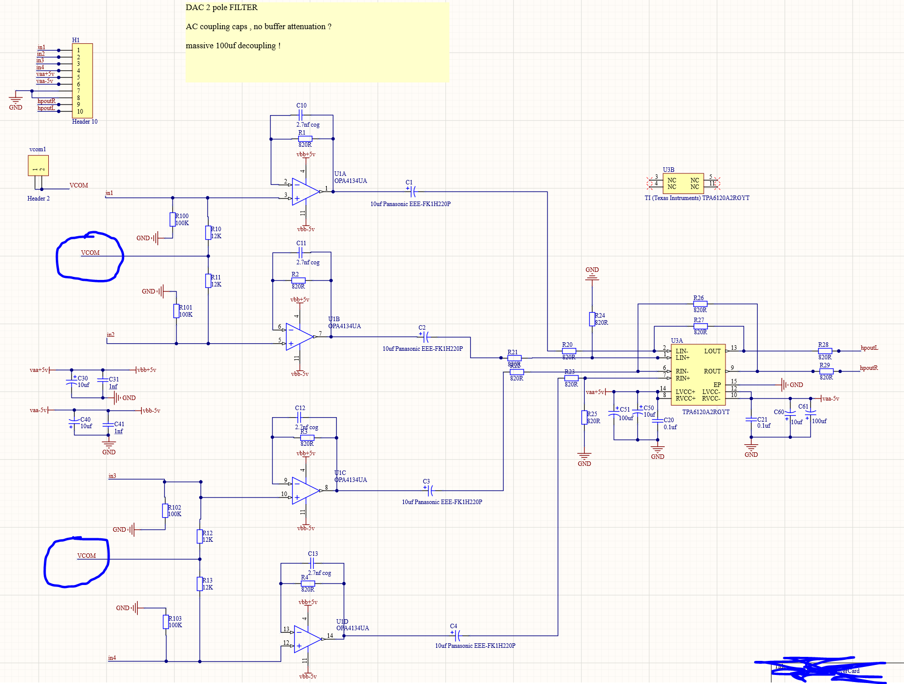
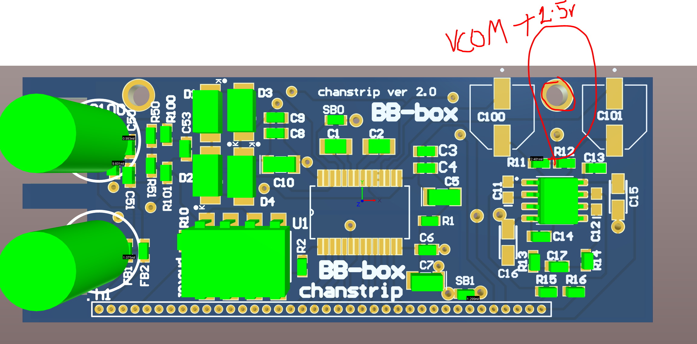
The preamps are working great with the new buffered VQ ( vcom ) going down a bolt that holds them in place.
I can't say the same for the headphone preamp at all !!
I had not really thought through the bias injection to the buffer properly ( tried to inject it into each input leg of the negative rail which has the negative feedback loop. the positive was going to GND ) wrong.
ignore the note about 100uF decoupling ! 10uF c1,c2,c3,c4 should be enough to remove the DC bias :)
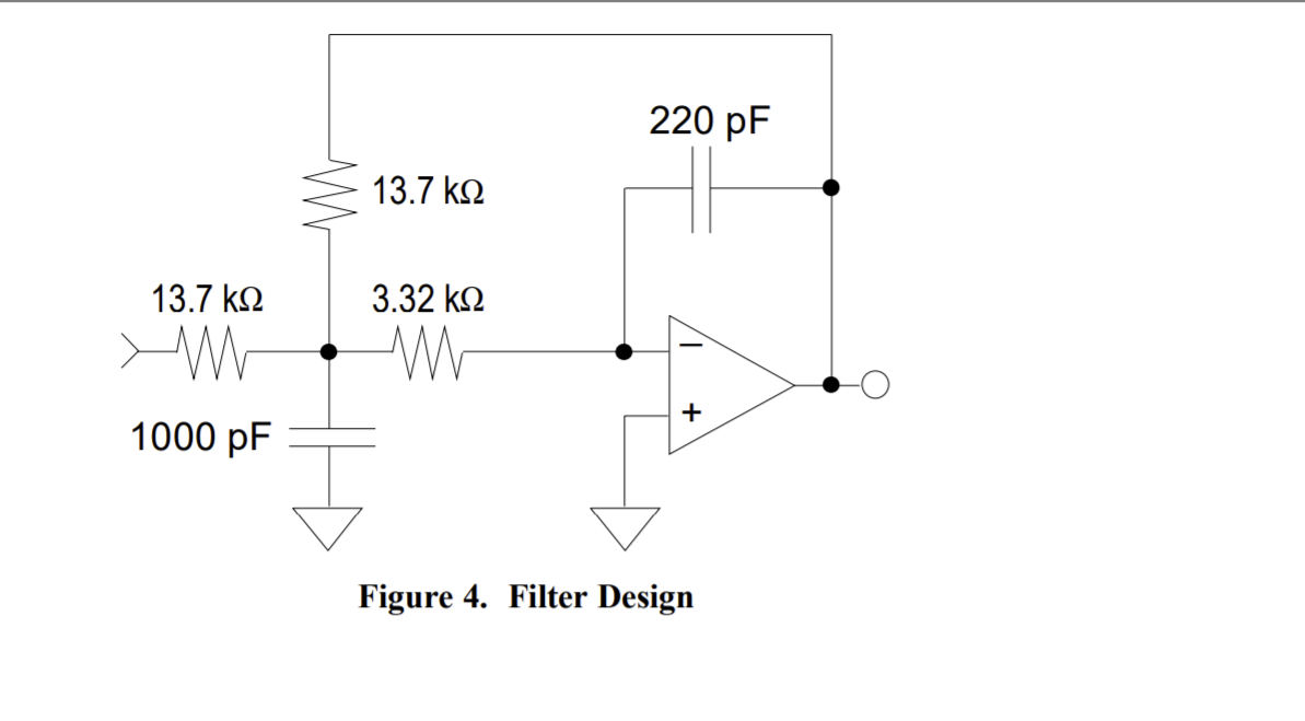
Now I need to incorporate this 50khz corner frequency filter in the negative feedback loop of my 4 channel OP4A134 or OPA1604 if this basic version works.
from a cirrus logic app note :
A two-pole Butterworth with a corner frequency of 50 kHz attenuates the signal at 20 kHz by approximately 0.1 dB and has nearly ideal phase linearity within the audio band
As I type this I realise it may have been more sensible to breadboard the buffer with the filter and test it 1st before sending off for the pcb..
I can test the filter with a sweep generated by the DSP from say 15khz -> 100khz and make sure the filter is doing the job.
I assume these ultra high frequency's can effect the lower ones harmonically if they are not removed? anyone know why i am actually making this filter ? it's just the recommended one in the datasheet !
I connect the differential DAC audio signals to the non inverting inputs of the 4 channel op amp IC and bias it with the buffered VQ (VCOM) form the DAC. I think if I need some attenuation of the DACS outputs I'll need to use voltage dividers on the inputs as the non-inverting inputs since any non-inverting op amp input has a minimum gain of 1 ? in other words in this configuration I cannot use the buffer for attenuation.
Please drop a message in the comments section if I am wrong there? thanks in advance :)
EDIT: I just realised I can set the output level of the DAC using I2C registers , so would never need to set attenuation anyway.
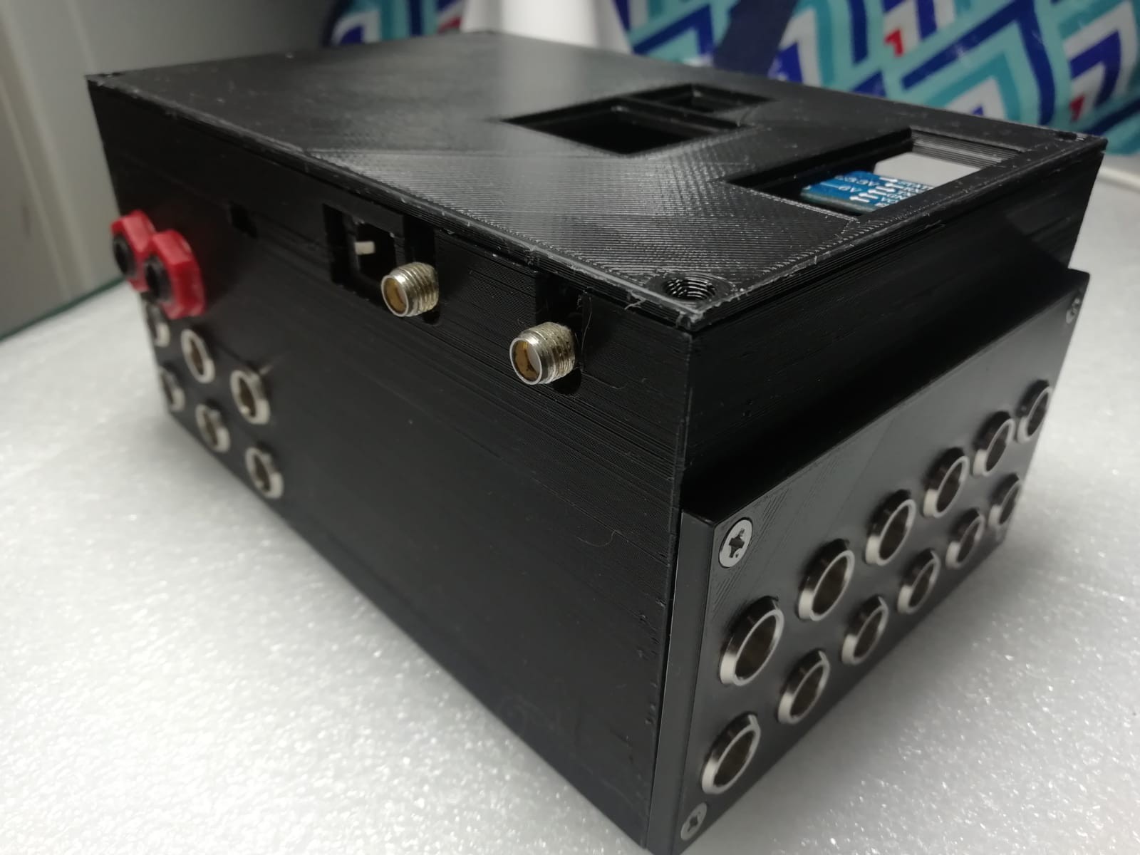
As you can see this is my 1st go with a 3d printer! It's actually my 2nd go at the lid. The 1st lid was completely wrong , always measure twice !
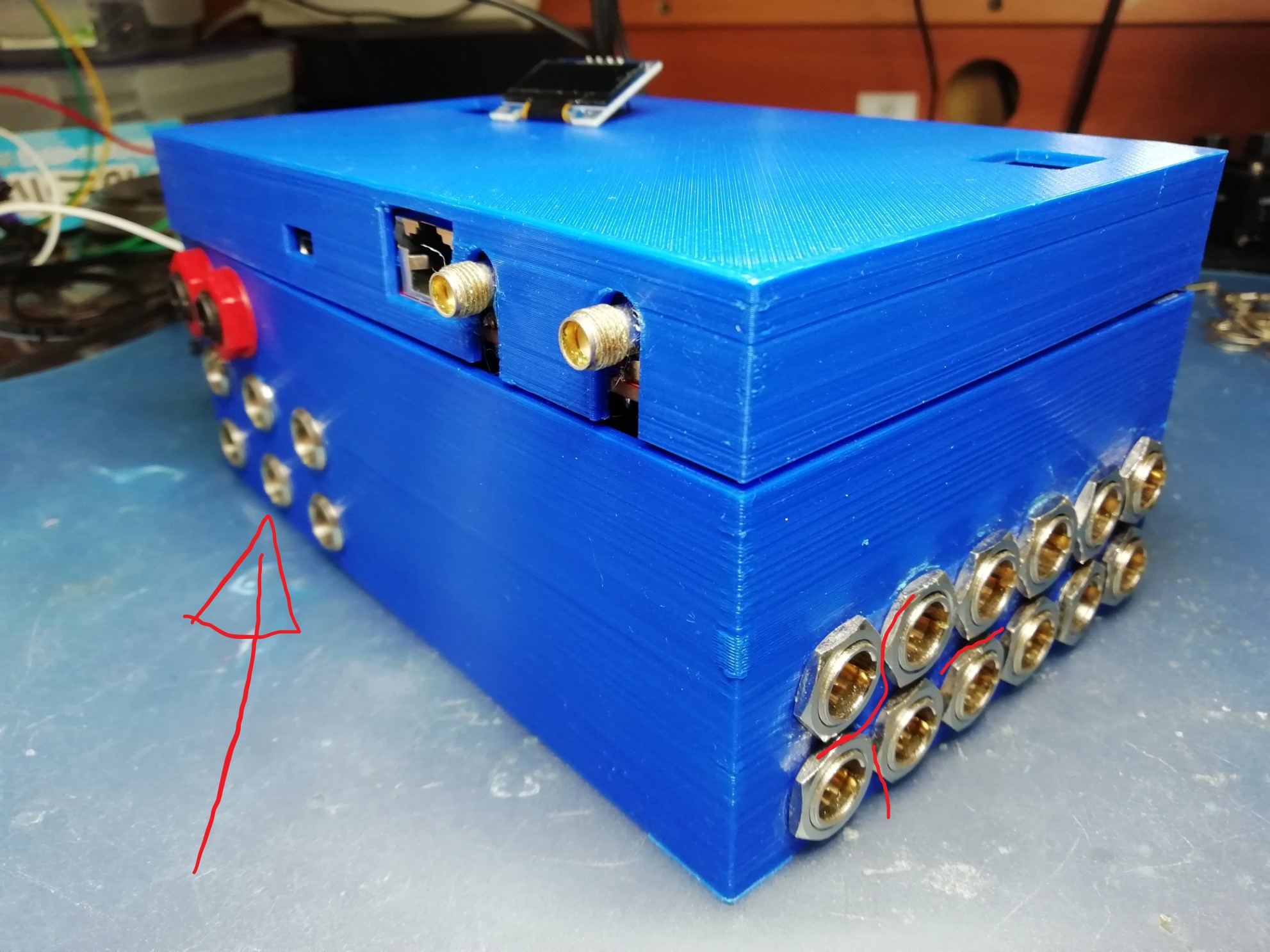
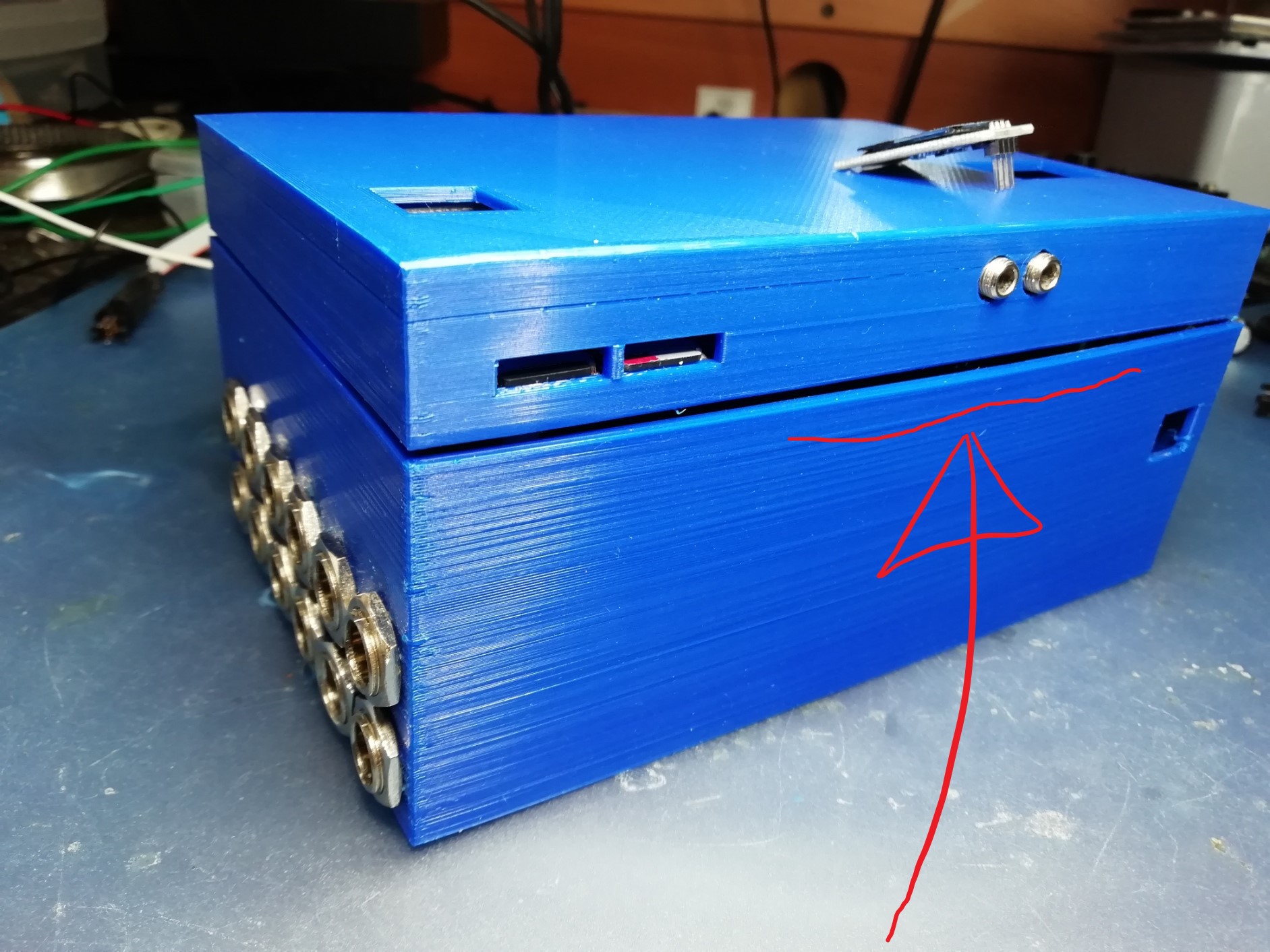
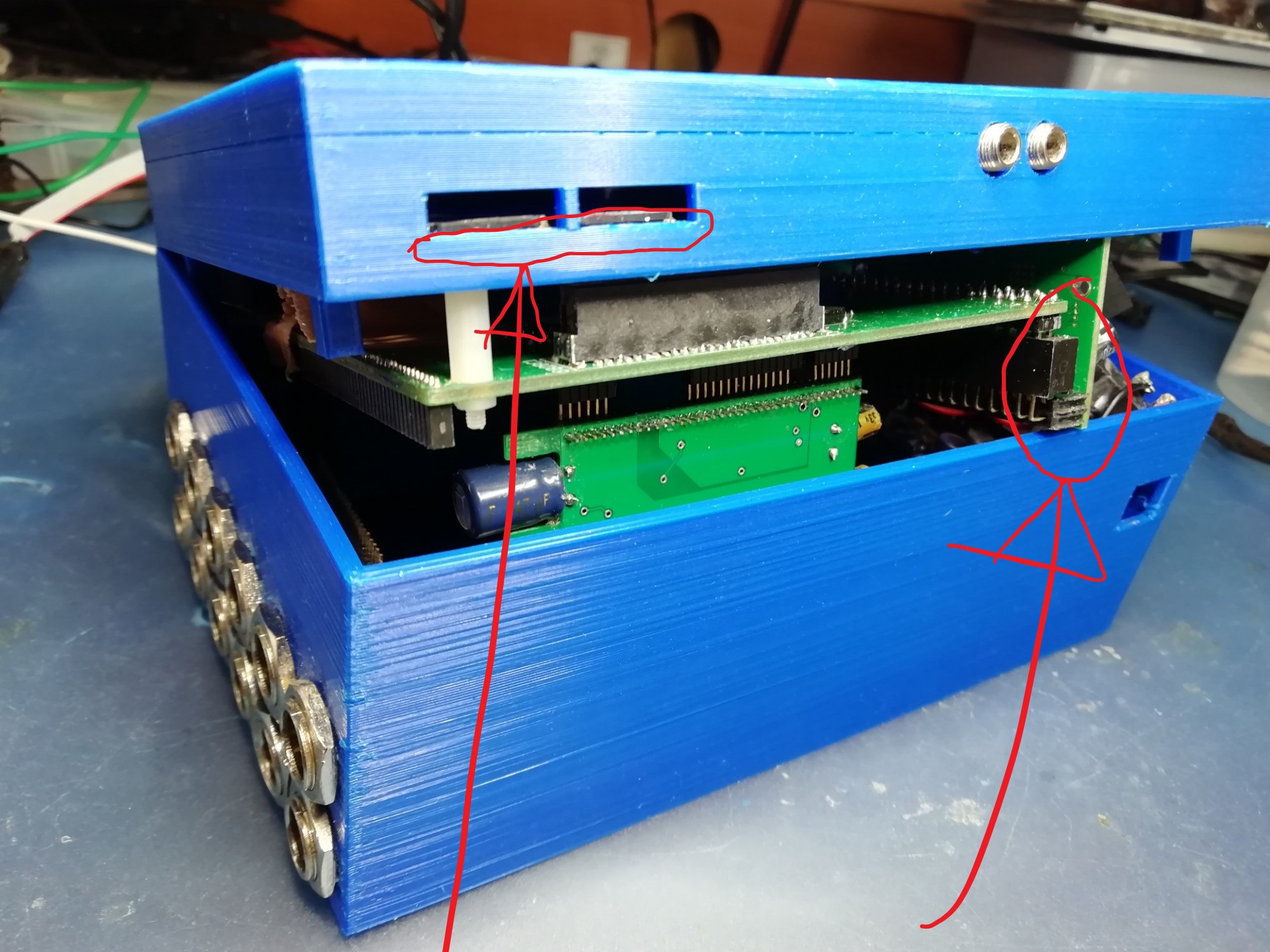
my specially ordered miniXLR sockets with the nuts on the outside of the case are stupid. I realised the pcb on the back is worth 1$ so it's far better to put the mini xlr sockets in through the holes ( should be D shape 11mm ) then tighten the nuts / washers from the inside the case before soldering the pcb onto all the pins. need to add thread lock glue to those nuts I think or you would end up with a bunch of washers and nuts flapping about in between the sock and pcb eventually.
cramped ugly nuts on the exterior of the case.. no ! got to go :)
top right corner it a whole for the programmer cable.
the uSD cards need more thumb room , it's a tweezer job to get them in and out !
The whole case needs beveled edges , way too sharp everywhere!
The bulge in the case is caused by the 40pin analogue board connector from ADC DAC card
that protrudes over the edge of the board edges. easy mistake to forget that those IDC connectors are much wider than the box around the footprint on the PCB !
for now I will just cut a whole in the case so it doesn't warp the box as I want to change the connector for light weight FPC ribbon cable , so its a problem that will eventually go away :)
Well I guess this is the great thing about having a 3d printer , you just keep refining the case until your happy then get it made professionally. I didn't bother with vase mode or whatever is the best way to print. I used sun PLA+ which is slightly stronger than the usual PLA. But could well have used anything.
time to do some work on the preamps and line driver cards now I have learned more !
Originally I tried to avoid using buffers between the ADC and preamps and DAC and line drivers.
not really my best idea ! I think I avoided them since I just didn't really know what they did :)
.. since then I have learned the PGA2500 vcom is in fact an input !!! pretty basic information but something I had completely overlooked.
There is an advantage of having the PGA's audio signals swinging around 0V so I had connected VCOM to ground.
BUT... the ADC has to swing around about 2.5v or near since it just used +5v. The exact bias voltage is available on VQ the pin.
you can't just hook up VQ to VCOM on the the pga or ADC buffer driver ( 10uA maximum current sink for VQ )
OK , I need a VQ buffer so I can send this bias reference across all 8 preamps.
why not just add a buffer / proper filter as recommended in the data sheet and keep the PGA2500 VCOM connected to 0V with decoupling capacitors in between the buffer biased at VQ ( buffered )
the buffered VQ bias ref voltage has to get around all the preamps !!
Staring at the cards and backplane it seemed like VQ was going to make a massive trip all over the design and pick up who knows what EMI.
Ages ago I thought at some stage I will need to add a threaded bar right through all the preamps to stop them flapping about in the header sockets. then I though , just send the VQ voltage down that bar.
then I briefly thought I had a clever idea , followed by another moment when I realised they have very likely been doing tricks like this since the days of vacuum tubes.. followed by another thought of , maybe the massive 2m threaded bar will pick up even more noise than if had just supplied the buffer with 2.5v from voltage dividers of the the 5V rail. The same 5V the ADC uses anyway.
I don't know what's inside the ADC IC , how is VQ derived ? Its ridiculous to think it probably is just voltage dividers !
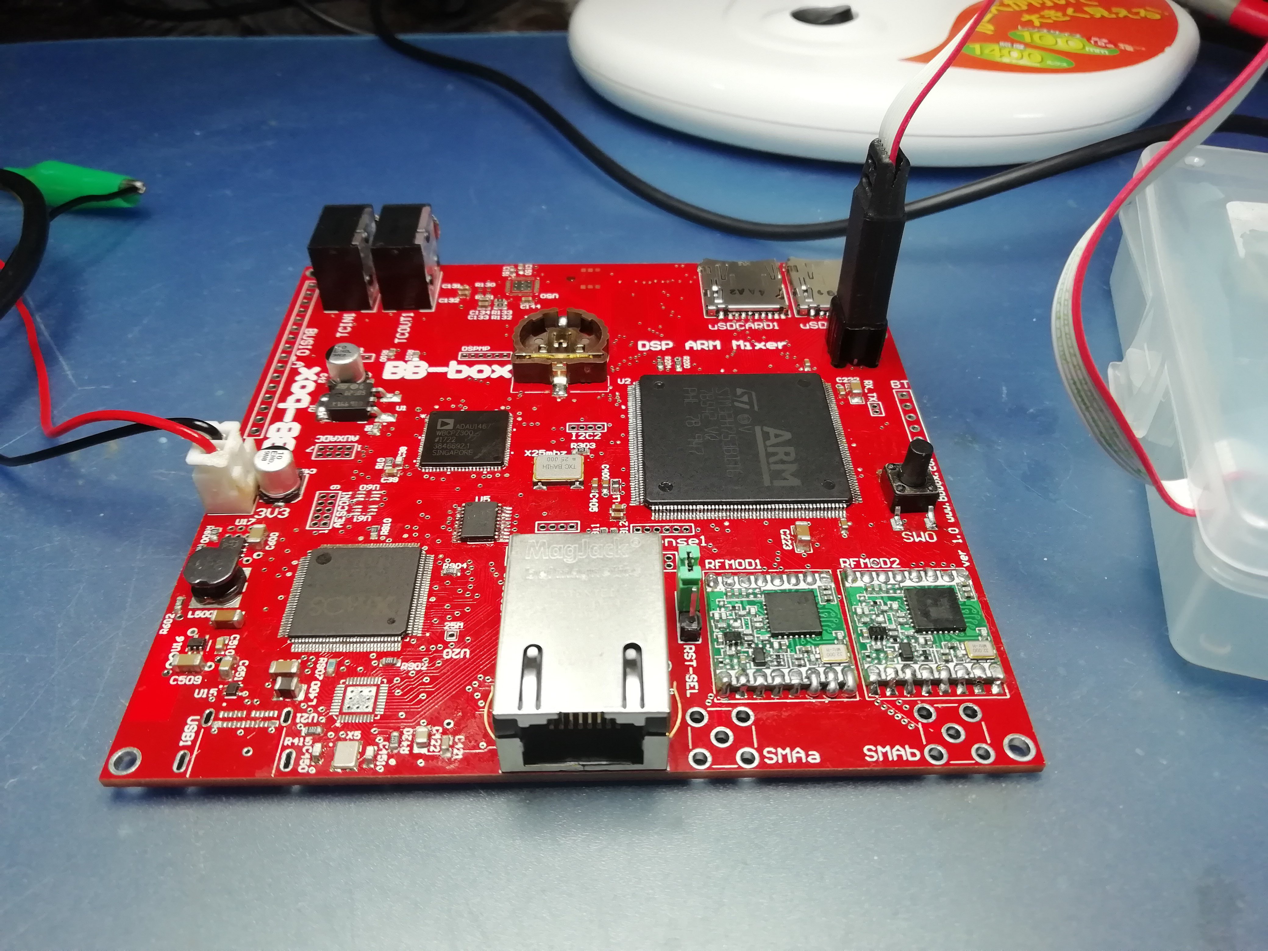
finally pretty much back where i started before the stm32f7 to H7 upgrade.
I still have an annoying bug in the BT app -> Micro where I need to press a button 3 times before it makes it to the app.. the sliders are probably only sending every 3rd value to. Its obviously a buffer or just the annoying fact I have no EOL character being recognised in the UART between stm32 and HC06 module.
I'm sure there is an obvious fix. I'm using DMA and streaming out tons of meter value data on the same UART. 10 characters go one way and 3 come in for device control. I did try and align the buffer of TX and RX but it didn't help. It could also be the way the App Inventor code sends the characters!
[edit]
Fixed ! as soon as i finished writing this log , I tried disabling the FIFO buffer on the UART and bingo.
one press on a button and instant reaction in the hardware. The sliders feel more accurate too since there not skipping values.
It's working with an interrupt that happens when 4 character arrive in DMA. my incoming commands are a fixed 4 bytes long. the 1st byte is just a marker to check I am receiving a real command and not garbage.
I don't send back any acknowledge byte yet to the app.
[end edit]
The individual channel power switching is working. I will need to force a mute on the powered down preamp channels as there is some small noise there. I can do that in the ADC or the DSP , not sure which is better , possibly better to mute the relevant ADC channel so it's quiet when powered back on. Now there is a large thud ( boom ! )
I don't really like the 1.27mm headers , pins can easily snap off and the connections are not as solid as 2.54mm. looking forward to the day I can just solder those preamp cards onto the backplane ! There is no way I would have got 8 preamp channels in such a small box with the larger headers so no choice ! I do wonder if I would have been better off using flat flex ribbon cables like in a mobile phone.
I think the next job after fixing the BT uart will be ltc timecode IO which will come through the TI Codec on SAI3. I'm really looking forward to that from a C code perspective. Then right after that I have to wake up the RTC TXCO and figure out how to jam sync incoming timecode to it :)
Way off into the future but hopefully before next year I will get the Xmos chip awake and get AES3 IO in and out of the DSP ! Hopefully I can setup TDM8 on the XMOS to sync up the the DSP as a slave without to much trouble.
AVB seams like pipe dreams now , but the gigabit ethernet PHY IC is there waiting and connected to XMOS.
I doubt USB C sound card mode will work at the same time as AES3 and AVB but who knows ! that will be decided by XMOS computational power and my coding ability in the XMOS IDE i think.
OK its all working fine so I just need to upgrade the micro to get another SAI channel add XMOS and gigabyte ethernet.. what could possibly go wrong ??
re-writing the firmware with new pins and DMA channels etc is done and its starting to come to life.
Bluetooth works and so does the 1" screen on i2c2 for debugging. The DMA channels initialize and the player pushes audio samples through the DMA channel etc.
Then I probe the FS / TDM line on the DAC and I can see audio on all 8 channels of the TDM line. FS is not changing according to the WAV file the player code is playing.
The player finds the sample rate in the WAV header and should change the SAI port clock according to the sample rate of the file. The TDM channel number should also change ( usually to 2 for normal stereo ) The Channels switch on in RECORD mode individually but no audio getting through to DAC yet. I still need to check SPI port to analogue preamps is actually working although the current draw goes up when i switch on preamp 1 so looks like it is!
I'm running the STM32H7 with external HSE TCXO at 25mhz as I did STM32 F7
The player should change the SAI peripheral clock like this and it worked on stm32f7..
__weak HAL_StatusTypeDef BSP_AUDIO_OUT_ClockConfig(SAI_HandleTypeDef *hsai, uint32_t AudioFreq, void *Params){
RCC_PeriphCLKInitTypeDef rcc_ex_clk_init_struct;
// HAL_RCCEx_GetPeriphCLKConfig(&rcc_ex_clk_init_struct); // BEN do i need to run this ?
HAL_StatusTypeDef ret = HAL_OK;
/* Set the PLL configuration according to the audio frequency */if((AudioFreq == AUDIO_FREQUENCY_11K) || (AudioFreq == AUDIO_FREQUENCY_22K) || (AudioFreq == AUDIO_FREQUENCY_44K))
{
/* SAI clock config *//* Configure PLLSAI prescalers *//* PLL2_VCO Input = HSE_VALUE/PLL2M = 1 Mhz *//* PLL2_VCO Output = PLL2_VCO Input * PLL2N = 429 Mhz *//* SAI_CLK_x = PLL2_VCO Output/PLL2P = 429/38 = 11.267 Mhz */
rcc_ex_clk_init_struct.PeriphClockSelection = RCC_PERIPHCLK_SAI23;
rcc_ex_clk_init_struct.Sai23ClockSelection = RCC_SAI23CLKSOURCE_PLL2; // SAI23 clock selection !!! SAI2 shares peroph clock with SAI3?
rcc_ex_clk_init_struct.PLL2.PLL2P = 38; // PLL2P: Division factor for system clock. Min_Data = 2 and Max_Data = 128
rcc_ex_clk_init_struct.PLL2.PLL2Q = 1;
rcc_ex_clk_init_struct.PLL2.PLL2R = 1;
rcc_ex_clk_init_struct.PLL2.PLL2N = 429; // PLL2N: Multiplication factor for PLL2 VCO output clock. Min_Data = 4 and Max_Data = 512
rcc_ex_clk_init_struct.PLL2.PLL2FRACN = 0;
rcc_ex_clk_init_struct.PLL2.PLL2M = 25;
if (HAL_RCCEx_PeriphCLKConfig(&rcc_ex_clk_init_struct) != HAL_OK)
{
ret = HAL_ERROR;
}
}
else/* AUDIO_FREQUENCY_8K, AUDIO_FREQUENCY_16K, AUDIO_FREQUENCY_48K, AUDIO_FREQUENCY_96K, AUDIO_FREQUENCY_192K */
{
/* SAI clock config *//* Configure PLLSAI prescalers *//* PLL2_VCO Input = HSE_VALUE/PLL2M = 1 Mhz *//* PLL2_VCO Output = PLL2_VCO Input * PLL2N = 344 Mhz *//* SAI_CLK_x = PLL2_VCO Output/PLL2P = 344/7 = 49.333 Mhz */
rcc_ex_clk_init_struct.PeriphClockSelection = RCC_PERIPHCLK_SAI2;
rcc_ex_clk_init_struct.Sai23ClockSelection = RCC_SAI2CLKSOURCE_PLL2; // // SAI23 clock selection !!!
rcc_ex_clk_init_struct.PLL2.PLL2P = 7; // PLL2P: Division factor for system clock. Min_Data = 2 and Max_Data = 128
rcc_ex_clk_init_struct.PLL2.PLL2Q = 1; // PLL2Q: Division factor for peripheral clocks. Min_Data = 1 and Max_Data = 128
rcc_ex_clk_init_struct.PLL2.PLL2R = 1; // PLL2R: Division factor for peripheral clocks. Min_Data = 1 and Max_Data = 128
rcc_ex_clk_init_struct.PLL2.PLL2N = 344; // PLL2N: Multiplication factor for PLL2 VCO output clock. Min_Data = 4 and Max_Data = 512
rcc_ex_clk_init_struct.PLL2.PLL2FRACN = 0;//PLL2FRACN: Specifies Fractional Part Of The Multiplication Factor for PLL2 VCO It should be a value between 0 and 8191
rcc_ex_clk_init_struct.PLL2.PLL2M = 25; // PLL2M: Division factor for PLL2 VCO input clock. Min_Data = 1 and Max_Data = 63if (HAL_RCCEx_PeriphCLKConfig(&rcc_ex_clk_init_struct) != HAL_OK)
{
ret = HAL_ERROR;
}
}
return ret; // should return HAL_OK
}
The clock RCC_PERIPHCLK_SAI2 = RCC_PERIPHCLK_SAI23
shared peripheral clock between SAI 2 and 3 ! !!!
I'm slowly getting there, but I'm wishing I included some easy hook onto probe pins now between on TDM lines between MICRO and ADAU1467 and perhaps TDM between XMOS and DSP ! of course that's easier said than done on a 4 layer board with so many signal lines.
The next job is to step through the code and check the TDM active slot number is being adjusted as it was in STM32F7.
the new board powered up OK and the debugger talks to the new STM32H7.
The H7 has more SAI ports
I'm using the 3rd port for the TI audio code for LTC timecode IO
The 4th port doesn't really configure in cubeMX as I've maxed out all the DMA channels !
my main mistake so far i can see is I don't have the XMOS I2C as slave connected up to the an i2C master on the STM32H7 in the way i was going to. somehow slipped through the net! the only use i could think for it was to shut down the XMOS chip for power saving anyway when not using AVB gigabit audio and/or aes3 and/or usbC pc mac connectivity. I find it hard to believe that little XMOS will cope with doing all three AES3 / USBC / AVB simultaneously but it's wired up like that in case :)
I made a little 2.54mm 20pin -> 1.27mm 20pin connector convertor for the XMOS debugger to save board space.
I'm still waiting for the TI codec IC / gigabit PY chip / RF connectors and USB C connector.
I'm pretty excited to be able to use the interface with a DAW over AVB or USB C.
In some ways it will be easier to test the analogue stuff without pulling the mico SD card out and inserting into the computer all the time !
One thing I should have included maybe is another USB socket to mount the micro SD cards from PC/MAC but i don't think that will be to hard to add in future revisions.
I need to also see if it's possible to add an SSD controller to an STM32H7. I imagine your moving towards having to run an operating system for that which i'm not really up for ! but if i can mount an SSD like the micoSD with a simple exFAT capable library in C then why not.
OK, lots of firmware work ahead after I update the analogue board and click together with the board to board connector :)
I will hopefully be able to reuse most of my code from stm32f7 but this time i'm using generated code from cubeMX and going to try adding my code in the user sections.. might be a trap ! herd horror stories of code being over written by cubeMX in user sections on forums so will have to make a lot of backups !
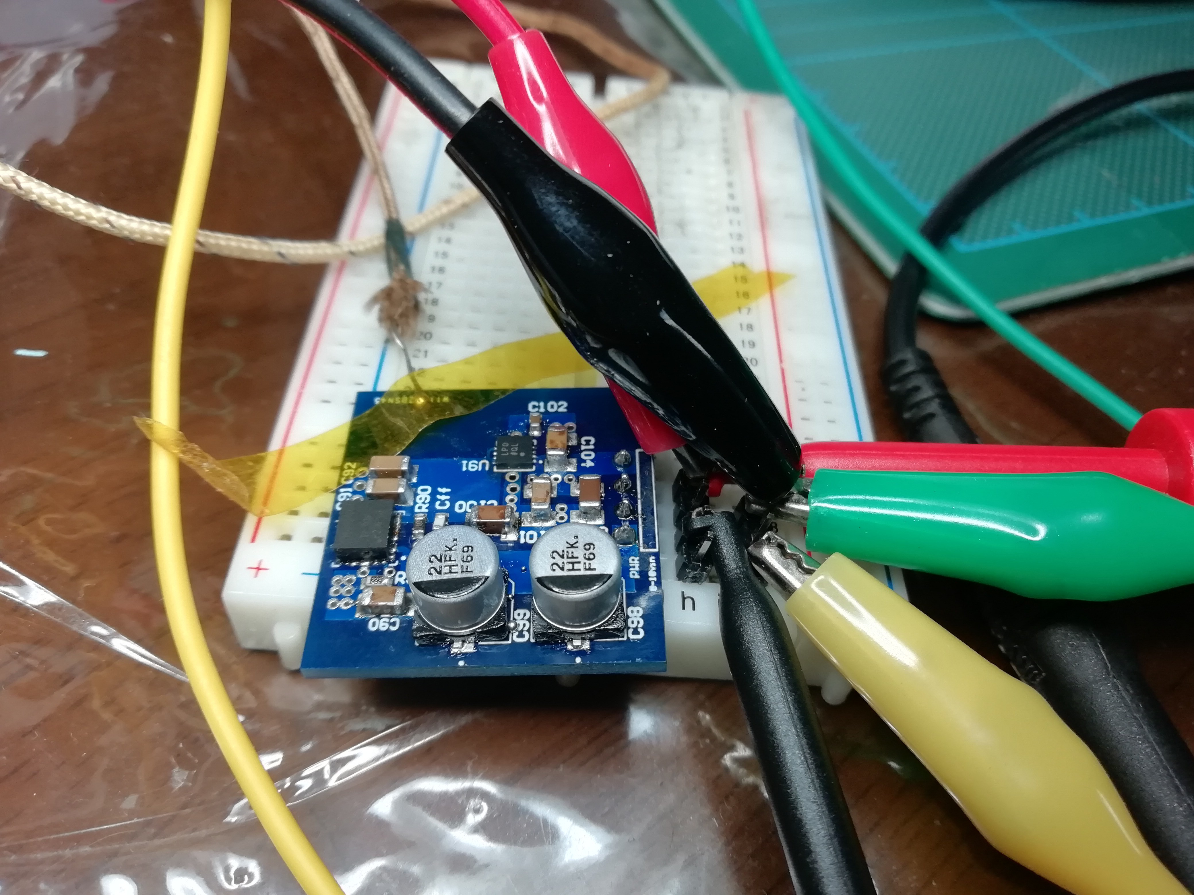
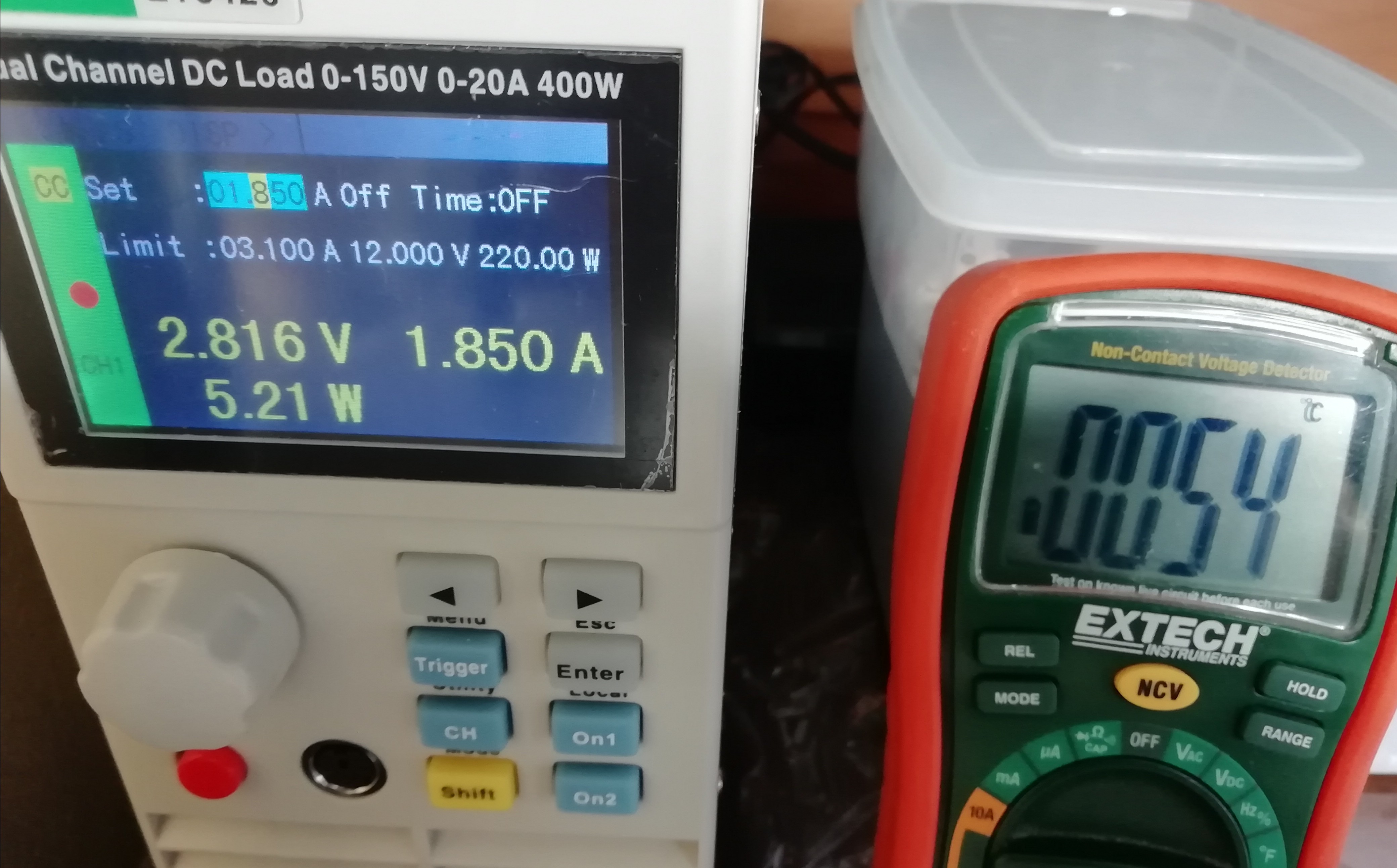
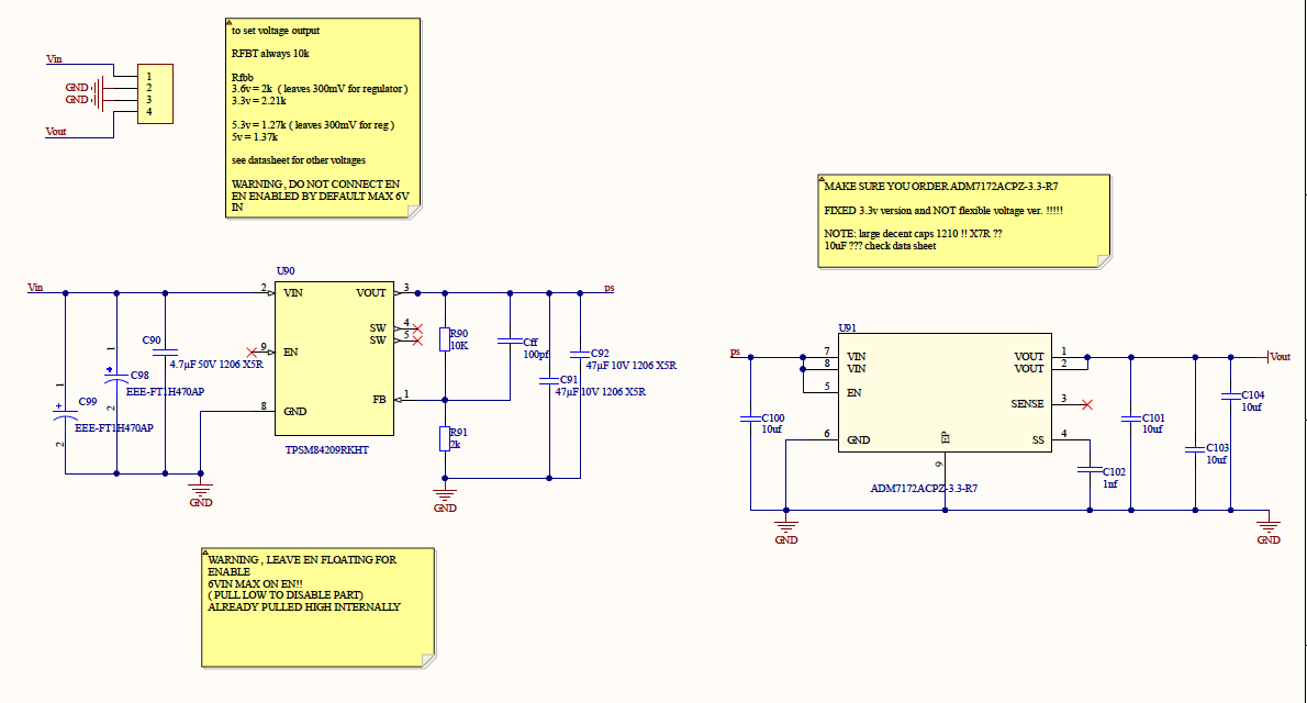
I just soldered up my new 3.3V 2A module and i'm running a test under load.
l2V supplyoutputthermo1.850A load and 3V out
the board temp is about 50c - 55c after an hour. ambient room temp is about 26c
the TPSM84029 4.5V - 28V input
ADM7172 fixed 3.3V output ( should be ! )
The dummy load is always a bit off so I hooked up my bench multimeter and noticed the voltage creeps down from 3.3 to 3v from around 1.25A load.
I'll never draw more current that around 1.2A and at startup only with the STM32H7 ADAU1467 and XMOS chip. but i'm interested in what can cause the voltage drop at the higher current draw?
at 1.25A 3.3V output 12Vin the board is at 40C
I really need to get an ESR meter I think to check the ESR of the input output capacitors.
Can anyone else see anything else wrong with my design ?
should I have more than 300mV headroom for the low noise LDO AD7172 ?
Could it even be at higher current loads multimeter test wires need to be shorter?
either way this module is way more stable than my last effort and totally usable in the design for now :)
 ben biles