 Saaddin
This project log is explaining about proposed schematics of The Low Voltage Translator and their simulation performance on TINA-TI SPICE. The proposed schematics of The Low Voltage Translator are shown in Figure 1 and Figure 2.
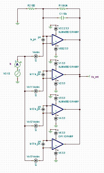
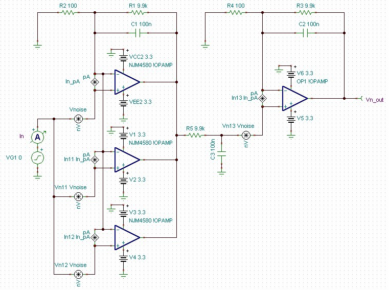
Because we only using low resistance value on the both schematic, we only considering input voltage noise and neglected the input current noise of the amplifier [1]. The total Gain in the 1st version amplifier is 1000 and the 2nd version is 10000.
The parallel configuration of the op-amp can reduce noise with the factor of 1/(sqrt(total of the parallel op-amp)) [2]. Since 1st version amplifier containing 4 parallel op-amps and 2nd version amplifier containing 3 parallel op-amps, so the 1st version winning the parallel effect for reducing noise.
In multiple stage amplifier configuration, the first stage of the amplifier add noise more significantly [3]. Therefore, in 2nd version amplifier 3 op amp on the first stage is parallel to reduce voltage noise in the first stage of the amplifier. The higher order low pass filter can reduced noise than lower order filter because the noise voltage in input op amp is white and can be reduced with more narrow bandwidth [3]. The multiple stage configuration amplifier like in the 2nd version enabling to apply higher order filter than in the single stage amplifier configuration like in 1st version. So, the 2nd version winning the filter effect for reducing noise with the 3rd order low pass filter.
To know about the best-proposed design, we simulate them in TINA-TI. Before doing the simulation, we make the identical model for JRC4580 in TINA-TI. The voltage noise density of the JRC4580 referring to its datasheet and the JRC4580 model in TINA-TI is shown in Figure 3 and Figure 4.
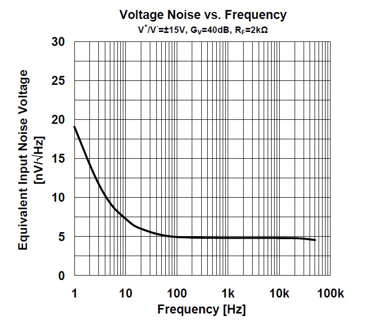
Figure 3. Noise voltage input density of JRC4580 from its datasheet
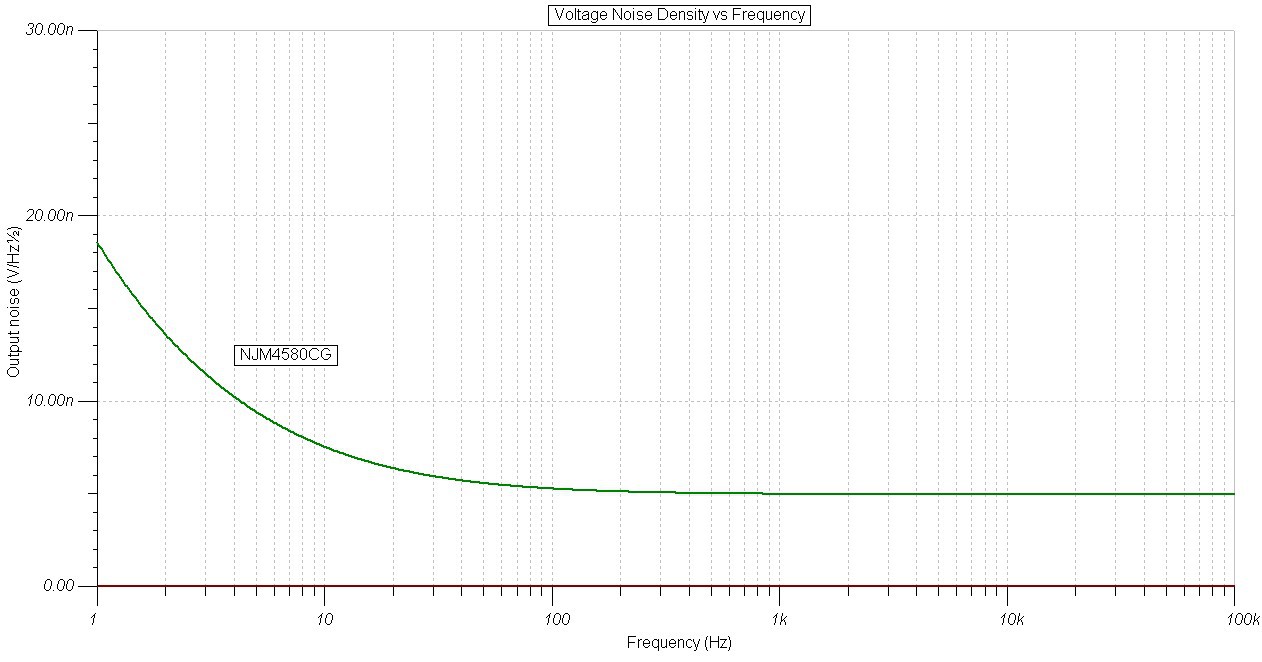
The Figure 3 and Figure 4 shows that the model of JRC4580 in TINA-TI is identical enough to its datasheet. The result simulation is the plot of RMS Noise voltage output vs Frequency on the 1st and the 2nd version of The Low Voltage Translator amplifier which is shown in Figure 5 and Figure 6.
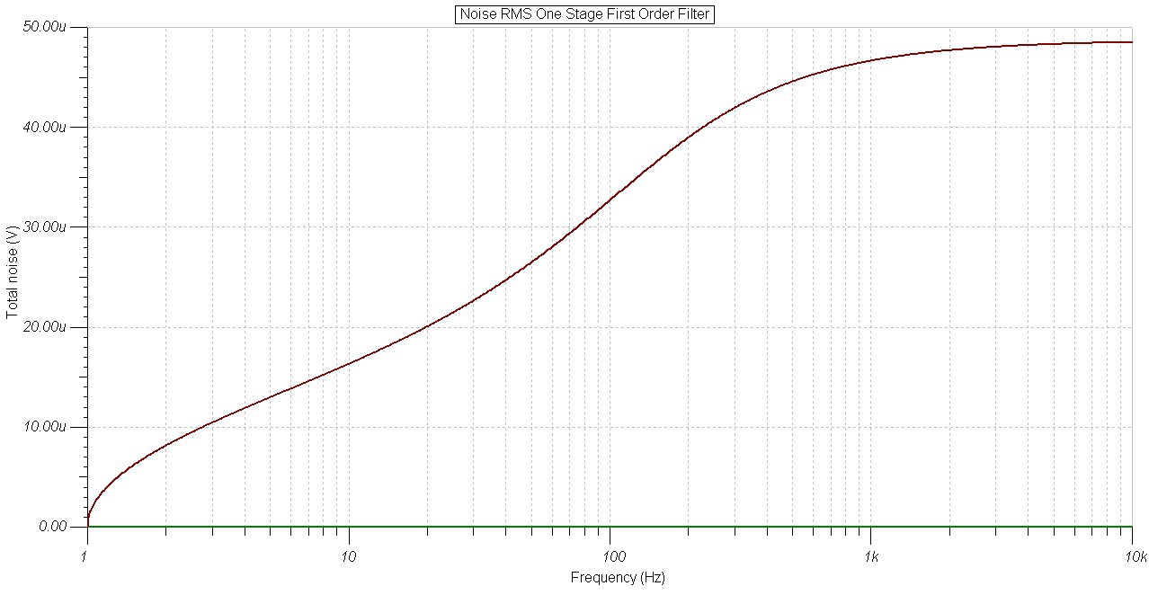
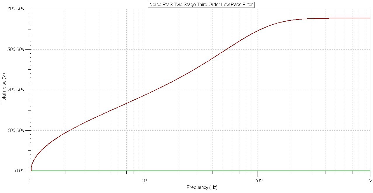
Figure 6. Simulation result of The 2nd version amplifier schematic
The magnitude of the vertical axis in Figure 5 and Figure 6 is Total voltage noise output amplifier in RMS. We need to divide those value with the gain of each amplifier to get voltage noise input in RMS. The result is 48uV/1000 = 48 nV RMS for the 1st version and 370uV/10000 = 37 nV RMS for the 2nd version.
The 2nd version amplifier is winning because of combining all method to reducing noise. Because the meaning of VRMS of noise is the probability, we will use the approximation of 6 x VRMS = Voltage Noise peak to peak with 99.7% probability [4]. So, the value of Voltage noise input peak to peak of 2nd version amplifier is 6 x 37nV= 222 nV peak to peak. Since we want to detect 10uV, the 222 nV is about 2.5%. In the next progress, we will use this data to compare with the data from the prototype of The Low Voltage Translator using the 2nd version of schematic.
Reference
[2] Linear Technology, Corp. LT1028 ref. C. Datasheet.
[3] Kay, Art. Williams, Ian. TIPL1314, Noise-4 TI Precision Labs Op Amps. Texas Instruments.
[4] Kay, Art. Williams, Ian. TIPL1313, Noise-3 TI Precision Labs Op Amps. Texas Instruments.
Discussions
Become a Hackaday.io Member
Create an account to leave a comment. Already have an account? Log In.