 Ted Yapo
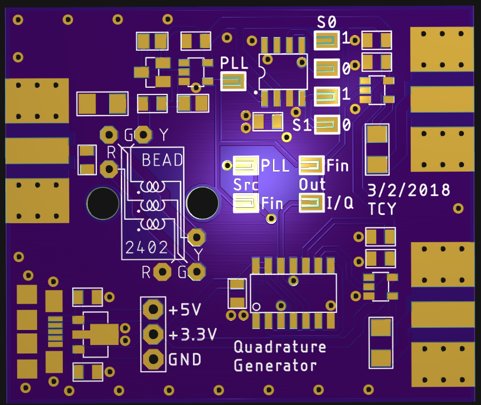
Here's the first design I just sent to OSH Park.
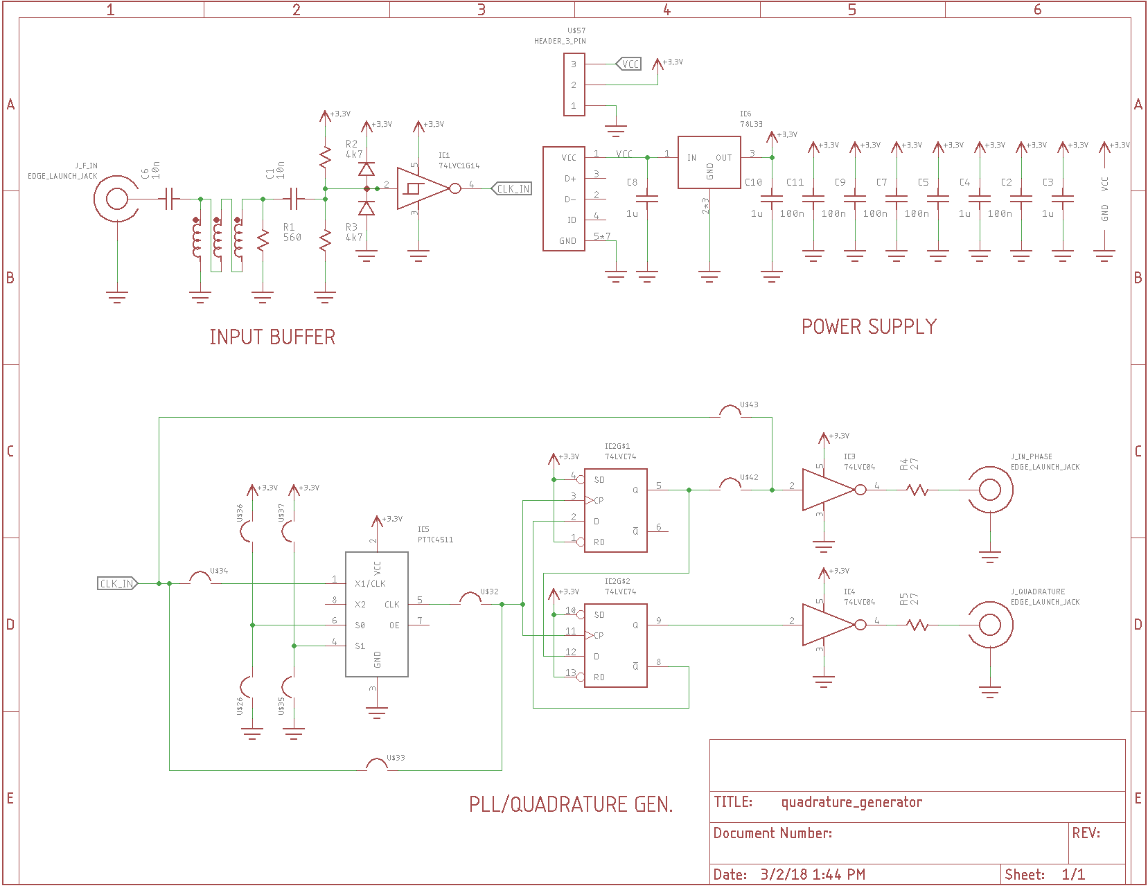
Input
The input jack connects to the tracking generator output of the DSA815. This output has a maximum level of 0 dBm, or about 632 mV peak-peak into 50 ohms. I threw together a quick circuit to transform the 50-ohm input impedance up to 450 and boost the voltage up enough to toggle a 74LVC1G14 Schmitt-trigger inverter. To check things out, I simulated the front-end in LTspice XVII. Here's the schematic (note that the component designators don't match the schematic above):
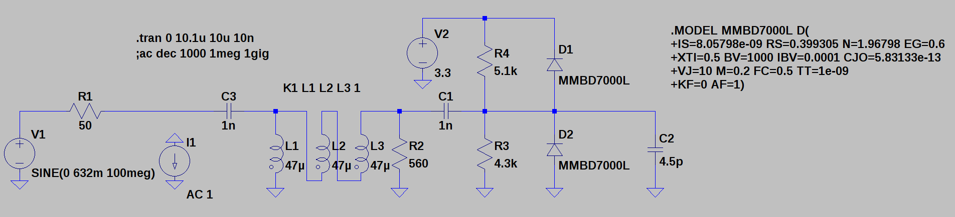
The input is assumed to have a 50-ohm impedance. C3 is included just in case I decide to drive this board from some source with a DC offset (like another clock signal). As a first guess, the transformer is 10 turns trifilar wound #28 Ga wire on a Fair-Rite 2643002402 core (43 ferrite material). It's sold cheap as a noise suppression core, but the electrons don't know this. Hams can substitute an FT37-43. I'll have to see how this core performs at 100 MHz and beyond. A different core material might be better.
The 1:3 turns ratio transforms the impedance up to 450 ohms, which is terminated with the three resistors in parallel. The 5.1k and 4.3k resistors bias the inverter input half-way in between the worst case high- and low-going input thresholds (1.5V). The dual diode protects the inverter input from ESD. These diodes are optional - they may not really be needed, and do alter the performance a little bit. The 4.5 pF capacitor represents the typical input of a 74LVC1G14 inverter.
I ran a transient simulation at 100 MHz. Note that the amplitude of the input voltage source (before back-termination) is 632 mV p-p, since it delivers 0 dBm into 50 ohms.
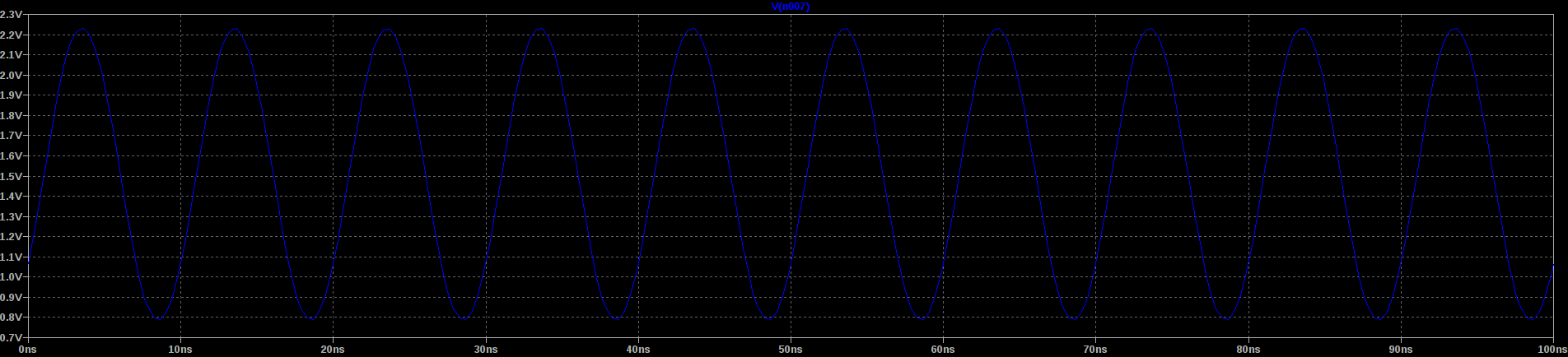
The output has peaks about 2.25V, and troughs of around 0.8V. The 74LVC1G14 isn't spec'd at 3.3V, but from the 3.0 and 4.5V specs, I estimate the worst case positive-going threshold to be 2.04V, and the negative-going, 0.95V. Just on the edge, really. At 10 MHz, the peaks are 0.6V and 2.4V, which looks better. Of course, the transformer simulation is very rough, so this is little more than an informed guess at this point.
Input Match
I also looked at the input impedance of the simulated circuit. You can see here that the input VSWR is 2:1 or less from around 1.8 MHz to 117 MHz.
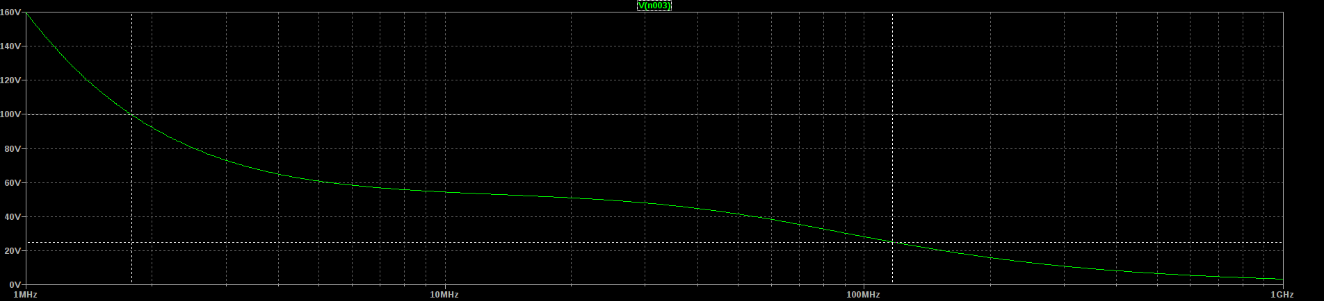
This is even more of a guess than the transient analysis above. It will be interesting to measure the input return loss of the assembled board and see how close it came.
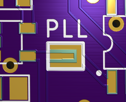
PLL
I added a clock-mulitplying PLL on the board for three reasons. First, I'm not sure how fast the front-end will go, and the PLL provides the option of a faster output clock than the input. I also wanted to be able to generate I and Q outputs at the same frequency as the input, which requires a 4x PLL. Finally, I just wanted to play with this particular PLL. It's a PT7C4511 from Diodes, Inc (was Pericom). It can output frequencies up to 200 MHz with 9 different multipliers, in this case, selected with solder bridges on the PCB.
Quadrature Generator
I used the classic Johnson-counter quadrature clock generator with a 74LVC74. It's supposedly good up to 200 MHz. There are solder bridges on the PCB for driving the clock from the input frequency or the PLL output.
Outputs
The I and Q outputs are driven from 74LVC1G04 inverters. The outputs are back-terminated with 27-ohm resistors, which I think will make 50 combined with the output impedance of the gates. I'll have to test this once the boards come back.
Power Ssupply
I added a micro-USB connector and 3.3V regulator as a power supply. The DSA815 has a USB port on the front which could be used for power (if I trust my PCB). Any USB supply should work. I also added header pins for 5/3.3V input or output.
Solder Bridges
I've used zero-ohm jumper resistors for board configuration before, but thought I'd try the cheaper solder-blob method this time. I made an Eagle component for this, and I can't wait to see how it works.
You should be able to blob some solder on there to close the "switch," or turn it off with some desoldering braid.
I sent the design off to OSH Park, so now I just have to order parts and wait for everything to arrive.
Discussions
Become a Hackaday.io Member
Create an account to leave a comment. Already have an account? Log In.
Love the preview images from your rendering program! We look forward to seeing more about this project
Are you sure? yes | no
Thanks!
So, it makes me wonder. Do you use the gerbv library for your board preview images? I use it to create the texture maps for rendering. Something causes these little gaps in solid fill areas. I haven't really investigated, but I suspect it's either a lack of sufficient decimal places in the gerbers to align each stripe perfectly, or roundoff errors in the gerbv rendering. I periodically get annoyed with this, but never quite enough to fix it :-)
Are you sure? yes | no
@Ted Yapo yes, we use gerbv. I'll ask @Dan Sheadel if he has any suggestions.
Are you sure? yes | no