0%
0%
Squidpad
Replace lots of stick notes and scraps of paper around the house with one Slim Quality Uncostly Intuitive Drawing Pad - [WIP]
 Arthur Admiraal
Become a Hackaday.io member
Already have an account? Log in.
Just one more thing
To make the experience fit your profile, pick a username and tell us what interests you.
Pick an awesome username
hackaday.io/
Your profile's URL: hackaday.io/username. Max 25 alphanumeric characters.
Pick a few interests
Projects that share your interests
People that share your interests
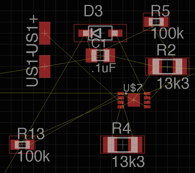
 I only had real trouble with soldering the connector for the e-ink display. In fact, I broke it in the progress. Luckily, I ordered two just in case. I have decided to wait with soldering this part until I have the microcontroller actually up and running, just to prevent my self from going insane because of one annoying connector.
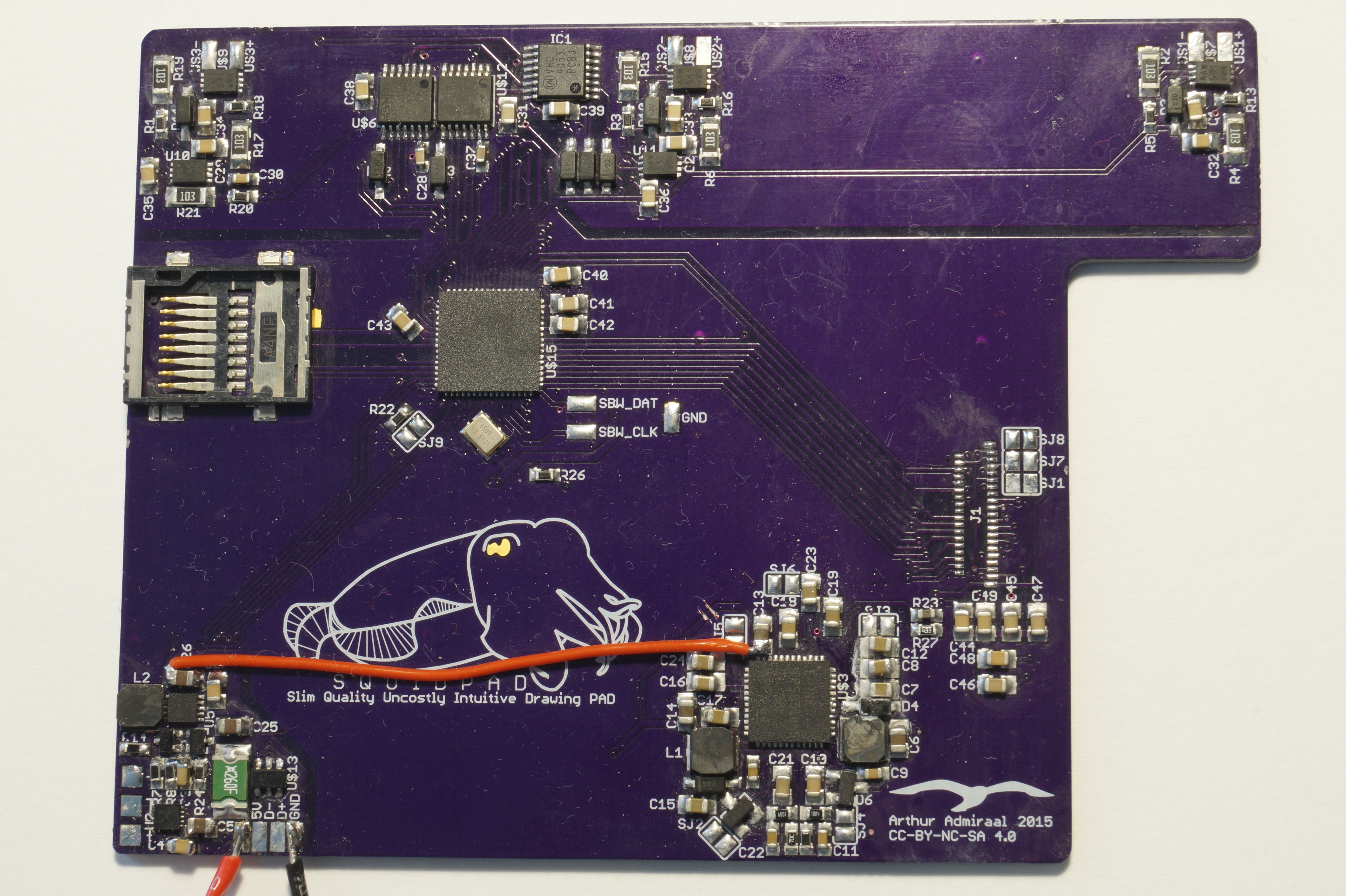


 Signal integrity
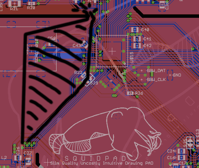


 Jovan
Jovan
 CriptasticHacker
 timonsku
 Matias N.
Very cool idea. A bit disappointing you couldn't pursue it further! As for it being a cheap solution I doubt that very much! I mean, how much does 500 sheets of paper cost? And they're a recyclable, renewable resource. That being said, I'm certain there'd be a future market for something like this and I'd be interested if it was rugged and robust and could also store your notes/drawings for transfer to PC.