 Arthur Admiraal
I thought it would be fun to tell a bit about my PCB design process.
I start out by loading in all the parts in the PCB editor. Often, my schematic is not complete at this stage, but I like to experiment with parts placement in advance.
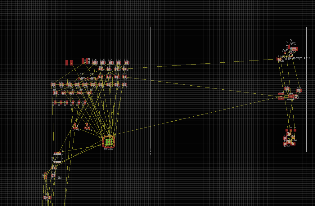
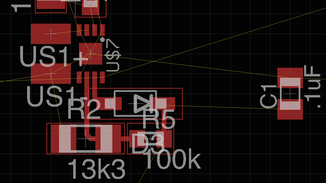
I then group parts by function. For example, the input amplifier is one small group.
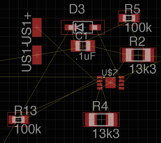
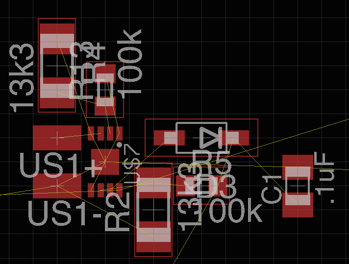
After that, I try to place the parts in such a way that the rats-nest wires are as short as possible.
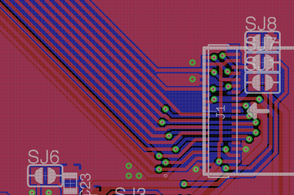
The next step is the actual routing. I often change the parts placement during routing, because I see a better way.
While routing, I still keep the power connections in mind, but I don't worry about it too much, as I often add a ground plane. I later add jumpers for any signal I couldn't route without them.
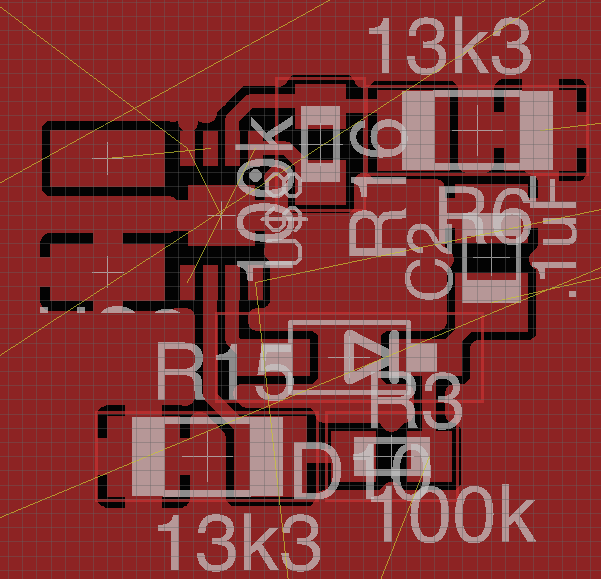
As a last step, I beatify the silkscreen, so that it is actually readable.
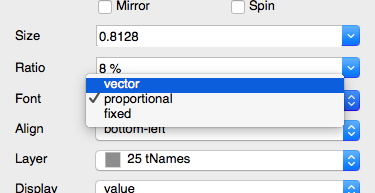
I delete all values of the components, as I can easily look them up in the schematic, or I could create a list for them. I set the text size to .8128mm (0.032"), which I think is the smallest silkscreen size that is still relatively readable when produced by cheap PCB fabs. I also switch the font to vector, as it is fixed and the fab won't change it from my design. I also sort of like its look. I keep the ratio at 8%.
Challenging parts
Prior to this project, I had actually never lain out a switching converter, so I stuck to the application notes as close as possible, and tried to make everything as compact as possible. I tried to keep the analog section as far away of the switching converters as possible, to minimize noise coupled into them from the relatively high currents in the converters. All the modules were joined to each other with big buses of wires.
I actually changed the signal net connections to the microcontroller to hugely simplify the routing.
Fitting everything together
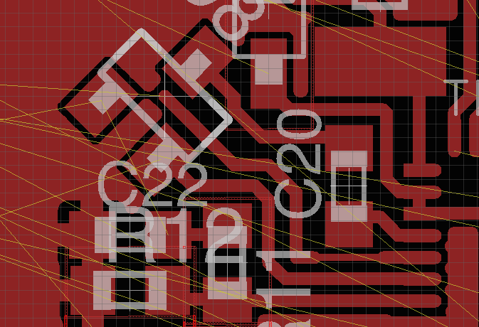
Because of the need to pack a lot of parts as close together as possible, it was sometimes challenging to route. To solve this, I briefly used thinner traces in some place. This technique is know as necking. Also, I rotated some parts 45 degrees to further assist in routing.
 Signal integrity
I haven't done much in the way of signal integrity in the past. This is the first project that I have actually consciously thought about it. I can't say that I'm an expert, but I tried some basic things to achieve better signal integrity.
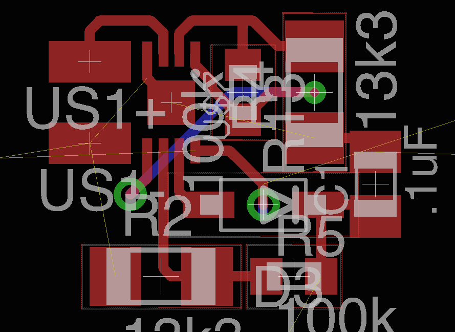
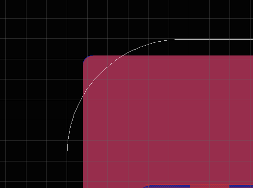
Apparently it is important to minimize the loop area of your traces. You see, the amount of energy picked up by a coil is proportional to the loop area. Switching power converters with their coils will generate quite a magnetic field. So, by minimizing the loop area, you minimize the noise picked up on the line.
Now, the loop area is the area between your signal trace and it's return path to ground. I've used some slits in my ground plane to hopefully force the current to go a certain way, in order to minimize the loop area. (Edit (24-april-2017): as pointed out by K.C. Lee in the comments below, forcing the current to go a certain way is not necessary for good return paths, but having the return path close to directly under the signal traces is, something which I have completely forgone on the right side of the picture below. He also suggested solving the problem using stitching vias. See his comment for more information.)
Looks like there might be a lot of noise on that power bus, guess I should have added some via's.
Other edits
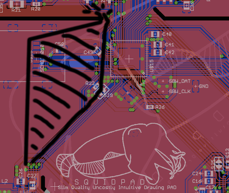
After getting all the circuitry perfectly laid out, I add my logo. I actually spend three full evenings getting my logo on the PCB. At first, I tried to use the svg2poly ulp, but because it doesn't support import of curved svg files, I had to subdivide the curves a bunch of times to make them look decent. Since eagle doesn't support polygons with a hole, I had to carefully divide my logo in multiple pieces. After two evenings of carefully assembling them, I sent my file to OSHpark, only to encounter a timeout. It turned out the svg-files had become too large. So I had to import my file as a bitmap and manually trace every detail of it. Not fun, especially since after the work of CERN on the module editor, a svg file can just be imported with a single click in KiCad. Why eagle, why!? (Edit (24-april-2017): cruz.monrreal, the author of the ulp, actually stepped in to explain why in the comments below, have a look if you are interested.)

Just before sending out my PCBs to be manufactured, I realised that I had the solder pads for the battery on the bottom of the PCB, while I had the components on the top. This meant that the PCB wouldn't sit flush in the enclosure, which would cost me an extra 0.2mm. Because of this, I decided to quickly change it to the other side.
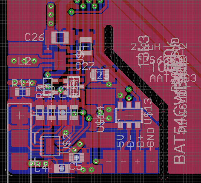
As a last touch, I rounded the corners of the PCB so that I can handle it more easily.
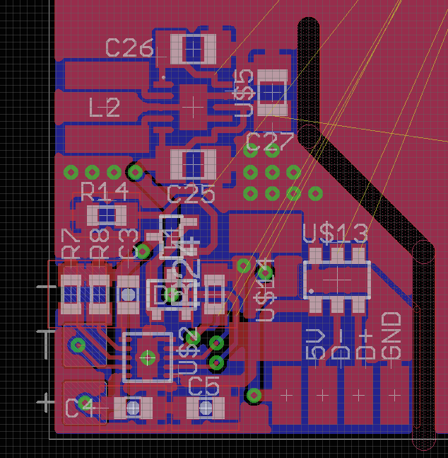
 I should mention that the PCB could be shrunk a lot, but since I wanted to minimize the risk of noise, I spaced out all the parts as much as possible. The big cutout in the PCB is needed to make room for the flat flex cable of the e-ink display. Oh, and I shared the PCB on OSHpark now so that it can be easily ordered. Click here to take a look at it. Alternatively, you can always look at PDF printouts on GitHub.
As of this log, the documentation is up to date with my development. Because of this, you won't see any logs for a while. This means that I will actually be able to spend some time refining the design of the enclosure, which I haven't had much time for because of the large amounts of time I spent documenting the project. But, I'll be sure to grab the keyboard whenever there is some significant new development, such as when I finally build my prototype.
Discussions
Become a Hackaday.io Member
Create an account to leave a comment. Already have an account? Log In.
>I've used some slits in my ground plane to hopefully force the current to go a certain way, in order to minimize the loop area.
You have a lot of the right words, but it doesn't show on your layout.
The best case to minimize the loop current is when the return path is running directly below the tracks on the ground plane just below it. i.e. the thickness of the PCB x the length of the tracks The return current will adjust itself to minimize the impedance by itself. There is no point of cutting slots to force the current flow. If you do want the slots, at least make the ground plane a bit wider than the signal tracks multiply a few times the thickness of the PCB.
I have seen and fix badly done split planes that causes more problems than it was supposed to solve.
Any time you cut a slot on the ground plane that is on the opposite side of the signal tracks, you are forcing the return current to go around.
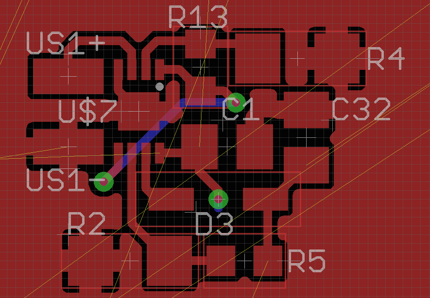
I have added the stitching vias (in big bright red dots) to the layout. Without the stitching, the return current path would have to travel towards the NW side on the ground plane. In reality, the return current would pick up a few of the neighboring signal tracks and this causes crosstalk.
Are you sure? yes | no
Thank you for your criticism! I will think twice about doing slots in future designs.
Coincidentally, I have just started my first course on electromagnetism which will hopefully allow me to have half of a clue about these things.
Are you sure? yes | no
Hey Arthur,
Sorry you had issues with the svg2poly tool. As for why it's not up to the same level as the KiCAD equivalent, the main reason is the Eagle Scripting Language itself. The KiCAD script uses Python as its backend, which means that it can use SVG libraries at it needs.
Meanwhile, in Eagle, I had to parse and decode the SVG itself, which is -incredibly- difficult when you have to build your own data structures as well. I'm still amazed that using a String as a fake Stack works as well as it does.
Are you sure? yes | no
Apologies for deriding your work. Thank you for creating the ulp with all those hacks-on-hacks you had to go through!
Are you sure? yes | no