 Howard Jones
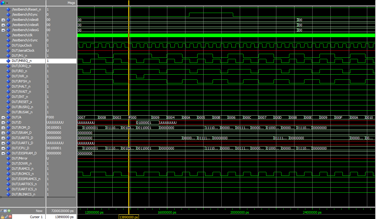
I fired up the project in ModelSim, and added all the Z80 and memory-related signals to it. From there I could see that memory requests in general were working OK, and could watch the Z80 pull bytes from ROM in low memory. I could also see where we got to the "LD (HL),A" instruction, that should update the display RAM at F000. F000 turns up on the address bus along with MREQ' and WR' and 65 on the data bus (a letter 'A' in ASCII). However, the chip select lines for the display RAM stay at 1 (off, it's active-low) and the request goes to the ROM instead.
Here's a picture of the problem. I think this stuff is really cool! Because your design is 'soft', you get a infinite-channel logic analyser for free... the DUT/A line is the system address bus, and DUT/DISPRAMCS_n is the display RAM chip select, with the others above it. At the yellow cursor, the Z80 has just asked for F000 - the actual write comes a clock later (clock at the top, WR_n a few lines below). Neat side note: You can also see the built-in Z80 DRAM refresh mechanism happening, which is why the address bus keeps jumping backwards and forwards - it's two sequences. One is driven by the Program Counter, and is fetching instructions, or data from memory with MREQ low, and the other is cycling through a 7 bit counter with RFSH low, to help you keep your DRAM refreshed. It does this while the rest of the processor is thinking about the current instruction, so the bus isn't required for memory or I/O access.
Anyway, knowing that the issue was with decoding, I noticed that I was comparing a 5-bit value to a 4-bit value for the display ram address decoding - something that the VHDL complier normally complains about - corrected that, and we were up and running!
For about 20 seconds.
Because now the address decoding is working, none of the RAM is optimised away, and the compiler has noticed that I still have dual-port, dual-clock RAM. Apparently, the same-size data buses isn't enough to fix it. So I lied - I told the system that I had the rev B fixed silicon. I actually have no idea if I do, because I can't figure it out from the label on the chip, but the symptoms are "possible memory corruption in certain circumstances", and since I have (mostly) one writer and one reader, I'm hopeful that I'll be OK. There is another workaround, but it uses twice as much blockram, and I don't have that to spare.
So the final exciting result:
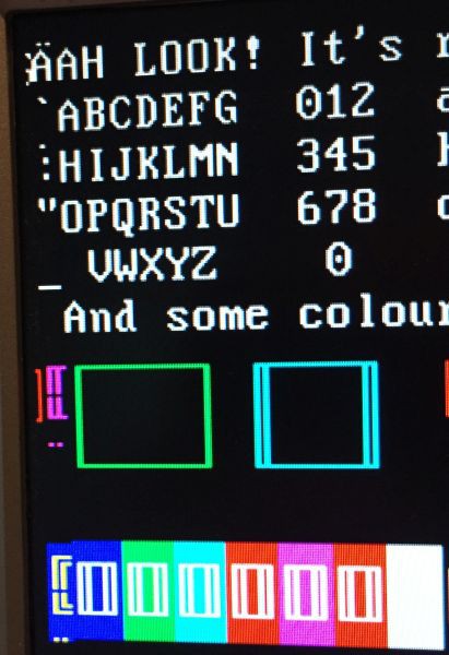
"AH LOOK" used to be "OH LOOK", and the "A" was put there by the Z80 software! It's not astonishing, but everything is talking now. Also, you can see the column-9 extension stuff working in the box graphics below it, to produce continuous horizontal boxes.
On to some slightly more advanced software to test i/o via the UART, a bit more virtual hardware to generate the 1.8432 MHz clock that the UART wants to generate baud rates, and some real physical hardware (MAX232 for now since I have one handy) to get the serial port to the right voltages to talk to other devices.
Discussions
Become a Hackaday.io Member
Create an account to leave a comment. Already have an account? Log In.