 novirium
To progress with the design of the electrical connection between modules, I figured I really just needed to start mocking things up and trying them. To that end, I drew up a rough version of an FPC jumper using the Molex SlimStack connectors I've mentioned before.
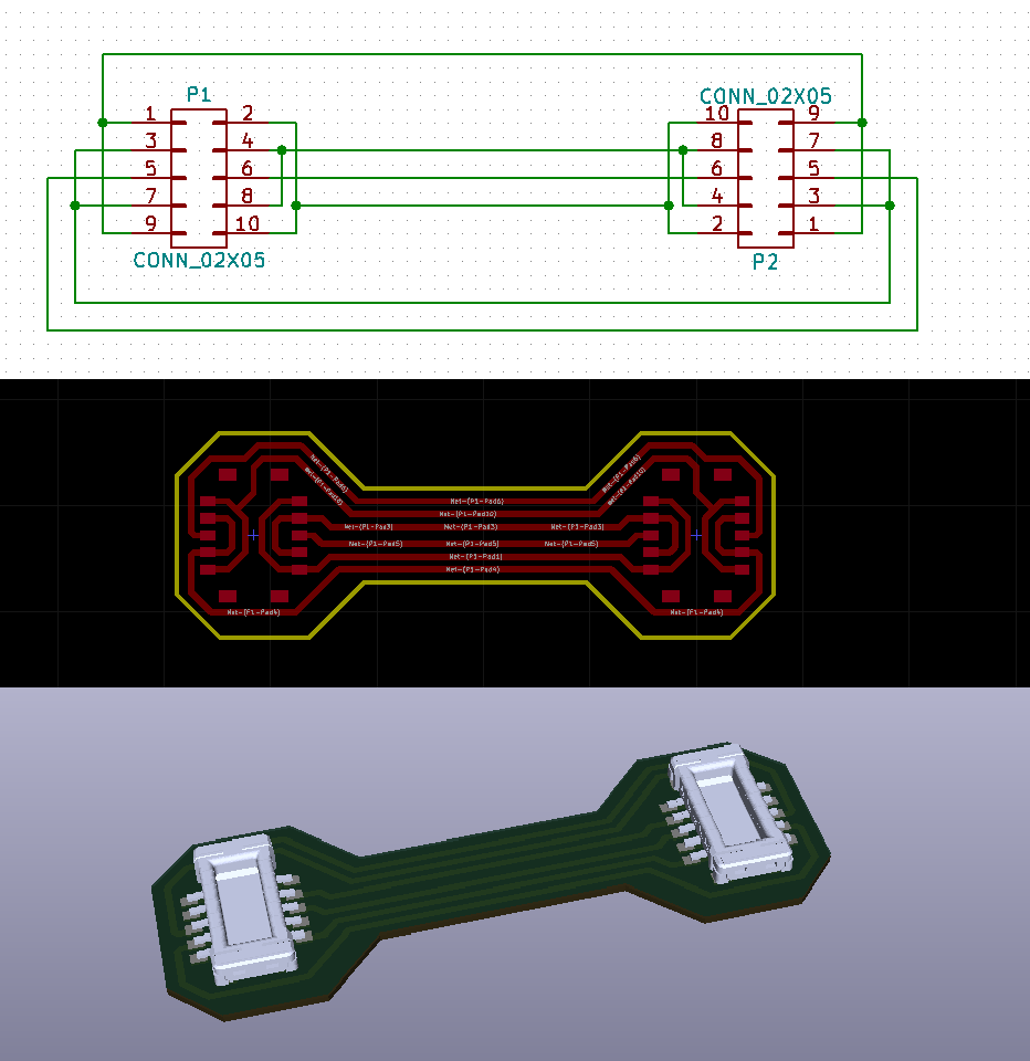 Though I haven't done any FPC design before, I'm aware that the rough design above needs a fair few changes, most notably curvier, smoother trace corners (honestly, a real pain in KiCad), and retaining pads leading out from the connector pads under the coverlay (also a pain).
The only cheap(ish) vendor I've found so far that offers a prototype service for FPC boards is Seeed Fusion. The list of design constraints for FPC on their site is pretty sparse though, so I sent them a support email explaining what I wanted to do, along with a copy of the gerbers for the strip shown above. If anyone is interested, apparently the minimum copper to edge distance is 0.2mm, and the required gerber stack is the same as their standard PCBs (no mention of a stiffener layer or anything). The reply also indicated they don't allow FPCs to be panelized, something that would be absolutely necessary for these small jumpers (it wasn't clear on what constitutes panelizing, I suspect having one large square and cutting them up with a craft knife would be fine). If anyone reading this has any other ideas as to where small jumpers like this could be made, please, let me know.
It turns out that getting the connections across the jumper while maintaining the rotational symmetry in the end connectors of the modules is a more complex problem than I'd first thought. 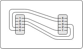 The simplest method is to use a basic 5 pin connector on the ends of the modules, and use a crossover jumper. As long as FPC is being used though, the design is ideally single sided. This means that there are at least 2 traces going around the edge of the connector, increasing the width of the jumper.
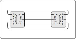 Almost all stacking connectors use two rows, and using a 10 pin double row connector instead allows for the design I used in the KiCad screenshots above. This layout adds another axis of symmetry to the connector, simplifying the design of the module PCB by allowing any of the connections to be pulled off either side of the connector. It does require a trace passing around each edge of the connector though (the screenshots above show a version that connects the center pins separately).
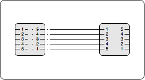 One other method I've found since then involves shifting the swapping of pins to the module PCB, allowing for a very compact jumper. Here the module PCB provides both pin orientations, one to each row of the connector, and one row on each end of the jumper is masked off, insulating it from the traces underneath. I'm not sure how successful this method would be, as it relies purely on the insulation of the soldermask (in the case of FPC, the coverlay) to separate the lines, and has fewer attachment points to hold the connector to the circuit board.
Discussions
Become a Hackaday.io Member
Create an account to leave a comment. Already have an account? Log In.